
Analog Devices Inc. ADP5040ACPZ-1-R7


- Part Number:
ADP5040ACPZ-1-R7
- Manufacturer:
- Category:
- RoHs:
 Non-RoHS Compliant
 - Datasheet:
- Description:
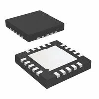
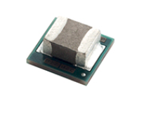
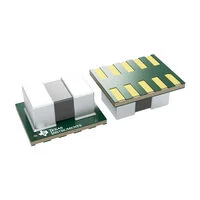
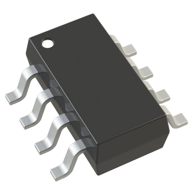
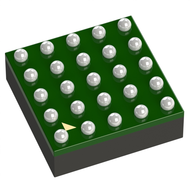
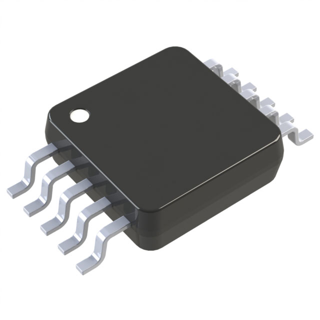
PMIC - Voltage Regulators - Linear Switching 3 Output Step-Down (Buck) Synchronous (1), Linear (LDO) (2) 3MHz 20-LFCSP (4x4)
- In stock 0

ADP5040ACPZ‑1‑R7: Micro PMU with 1.2A Buck & Two 300mA LDOs
1. Basic Information
- Manufacturer: Analog Devices Inc.
- Part Number: ADP5040ACPZ‑1‑R7
- Device Type: Integrated micro power management unit (PMU)
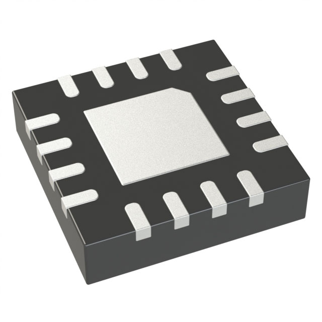
- Package: 20‑lead LFCSP, 4 mm × 4 mm, CP‑20‑8
- Marking: RoHS‑compliant; “Z” = lead‑free; “R7” = reel packaging
- Operating Junction Temp: −40°C to +125°C
- Storage Temp: −65°C to +150°C
- Revision: Rev. D
- UVLO Option: 3.65 V typical (Option 1)
- Active Pull‑Down: Enabled on all channels
2. Key Features
- 1 × high‑efficiency 1.2 A buck regulator
- 2 × low‑noise 300 mA LDOs (LDO1: digital; LDO2: analog‑optimized)
- Wide input voltage range
- 3 MHz fixed buck switching frequency
- Forced PWM or auto PWM/PSM mode selection
- 100% duty‑cycle low‑dropout operation
- Internal soft start
- Individual enable pins for each rail
- Comprehensive protection suite
- Tiny external components (multilayer ceramic caps/inductors)
- Low quiescent current for battery‑powered systems
3. Absolute Maximum Ratings
- AVIN to AGND: −0.3 V to +6 V
- VIN1 to AVIN, PGND to AGND: −0.3 V to +0.3 V
- VIN2, VIN3, VOUTx, ENx, MODE, FBx, SW to AGND: −0.3 V to (AVIN + 0.3 V)
- SW to PGND: −0.3 V to (VIN1 + 0.3 V)
- ESD HBM: 3000 V; CDM: 1500 V; MM: 200 V
- Max reflow temp: compliant with JEDEC J‑STD‑020
4. Electrical Specifications
4.1 General
- AVIN UVLO (Option 1): rising 3.9 V, falling 3.1 V
- Shutdown current (ENx = GND): 0.1–2 μA
- Thermal shutdown: 150°C (rising), 20°C hysteresis
- Buck startup time: 250 μs; LDO startup time: 85 μs
- Logic input: VIH ≥ 1.2 V, VIL ≤ 0.4 V (2.5 V ≤ AVIN ≤ 5.5 V)
4.2 Buck Regulator
- Input range: 2.3 V–5.5 V
- Output range: 0.8 V–3.8 V
- Output current: up to 1.2 A
- Switching frequency: 2.5–3.5 MHz (typ 3 MHz)
- Feedback voltage: 0.485–0.515 V
- Current limit: 1.6–2.3 A
- Peak efficiency: up to 96%
- PSM threshold: 100 mA
- Active pull‑down: 85 Ω
4.3 LDO1 & LDO2
- Input range: 1.7 V–5.5 V
- Output range: 0.8 V–5.2 V
- Output current: up to 300 mA each
- Feedback voltage: 0.485–0.515 V
- Output accuracy: ±3%
- Dropout voltage: 72–180 mV @ 300 mA
- PSRR: up to 66 dB @ 1 kHz
- Output noise: ~59–140 μV rms (10 Hz–100 kHz)
- Current limit: 335–470 mA
- Active pull‑down: 600 Ω
5. Protection Features
- Overcurrent protection (buck cycle‑by‑cycle; LDO current limiting)
- Thermal shutdown (150°C, auto‑recovery)
- Input undervoltage lockout (UVLO)
- Short‑circuit protection with frequency foldback (buck)
- Active output discharge when disabled
6. Pin Configuration & Functions
- AVIN: System supply (2.3–5.5 V)
- VIN1: Buck input
- SW: Buck switching node
- PGND: Buck power ground
- FB1: Buck feedback
- EN1: Buck enable
- MODE: Buck PWM/PSM control
- VIN2/VIN3: LDO inputs
- VOUT2/VOUT3: LDO outputs
- FB2/FB3: LDO feedbacks
- EN2/EN3: LDO enables
- AGND: Analog ground; EP: Exposed pad (must connect to GND)
- Pins 5, 18, 19, 20: DNC (do not connect)
7. Thermal Data
- θJA (20‑lead LFCSP): 38°C/W
- θJC: 4.2°C/W
- Max operating TJ: 125°C
- Exposed pad required for thermal performance
8. Application Information
8.1 Typical Applications
- Portable consumer electronics
- Battery‑powered devices
- Industrial & IoT sensors
- Low‑power microcontroller/processor rails
- Analog/digital mixed‑signal systems
8.2 External Components
- Buck inductor: 0.7–3.0 μH (1 μH recommended)
- Buck input cap: ≥4.7 μF (X5R/X7R)
- Buck output cap: ≥7 μF (10 μF recommended)
- LDO I/O caps: ≥0.7 μF (2.2 μF recommended for full load)
- Feedback dividers: set VOUT = VFB × (Rtop/Rbottom + 1), VFB = 0.5 V
8.3 PCB Layout Guidelines
- Place input/output caps, inductor close to IC
- Short, wide high‑current paths
- Dedicated ground plane; EP tied to GND with multiple vias
- Isolate SW node and inductor from analog feedback lines
- Maximize copper area for heat dissipation
9. Ordering Information
- ADP5040ACPZ‑1‑R7: −40°C to +125°C, 20‑LFCSP, UVLO = 3.65 V, active pull‑down enabled, RoHS, reel
- ADP5040CP‑1‑EVALZ: Evaluation board
Purchase
No need to register to order from JMBom Electronics, but signing in lets you track your order like a pro. Give it a try for a smoother shopping ride.
Means
Easy peasy! Pay your way with PayPal, Credit Card, or wire transfer in USD. We've got you covered.
RFQ(Request for Quotations)
Get the freshest prices and stock updates by asking for a quote! Our sales team will shoot you an email within a day. It's that simple.
IMPORTANT NOTICE
1. Look out for your order details in your inbox! (If it's missing, check the spam folder just in case.)
2. Our sales manager will double-check the order and keep you posted on any price or stock changes. No worries, we've got you covered.

Shipping Rate
We ship orders once a day around 5 p.m., except Sunday. Once shipped, the estimated delivery time depends on the courier company you choose, usually 5-7 working days.

Shipping Methods
We provide DHL, FedEx, UPS, EMS, SF Express, and Registered Air Mail international shipping.


Payment
You can pay the orders on the website directly or pay by wire transfer offline. We support: Paypal、VISA、Credit Card.


Analog Devices Inc.
Analog Devices Inc.
Analog Devices Inc.
Analog Devices Inc.
Analog Devices Inc.
Analog Devices Inc.

Analog Devices Inc.
Analog Devices Inc.
Analog Devices Inc.
Analog Devices Inc.
Analog Devices Inc.
Analog Devices Inc.