
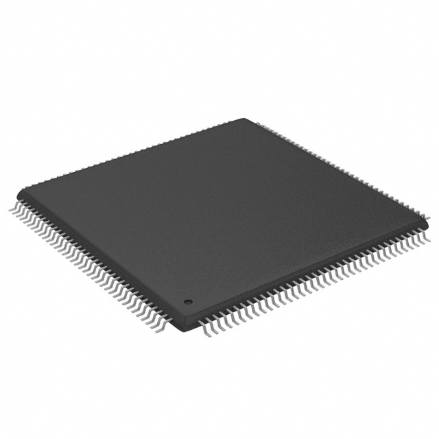
Alliance AS4C16M16SA-6TIN


- Part Number:
AS4C16M16SA-6TIN
- Manufacturer:
- Category:
- RoHs:
 RoHS Compliant
 - Datasheet:
 AS4C16M16SA-6TIN_Datesheet
 - Description:
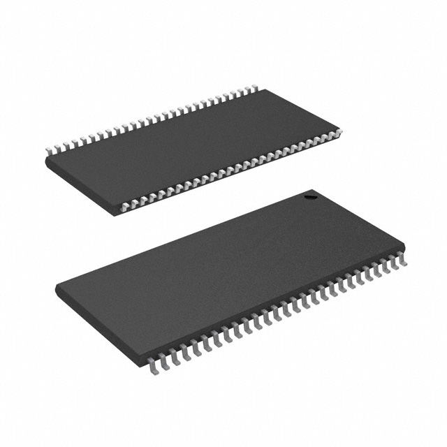
IC DRAM 256MBIT PAR 54TSOP II
- In stock 26,486

Model Information for AS4C16M16SA-6TIN
Basic Information
- Manufacturer: Alliance Memory Inc.
- Model Number: AS4C16M16SA-6TIN
- Document Number: DS36599 Rev. 3.0
- Date: March 2015
- Website: www.alliancememory.com
Description
The AS4C16M16SA-6TIN is a 256Mb (16Mx16bit) Synchronous DRAM (SDRAM) designed for high-speed CMOS synchronous DRAM applications. It features an internal pipelined architecture, programmable mode registers, and a wide operating temperature range suitable for industrial applications.
Features
- Fast Access Time: 5 ns (from clock)
- High Clock Rate: 166 MHz
- Fully Synchronous Operation
- Internal Pipelined Architecture
- 4 Banks of 4M words x 16-bit
- Programmable Mode Registers:CAS Latency: 2 or 3Burst Length: 1, 2, 4, 8, or full pageBurst Type: Sequential or InterleavedBurst Stop Function
- Operating Temperature Range:Industrial: -40°C to 85°C
- Auto Refresh and Self Refresh
- 8192 Refresh Cycles/64ms
- CKE Power Down Mode
- Single +3.3V ±0.3V Power Supply
- Interface: LVTTL
- Package: 54-pin TSOP II
- Compliant with RoHS and Halogen-Free Standards
Applications
- High-Performance PCs
- Graphics Cards
- Switching Power Supplies
- Industrial Control Systems
- Embedded Systems
Key Specifications
- Clock Cycle Time (tCK3): 6 ns
- Access Time from CLK (tAC3): 5 ns
- Row Active Time (tRAS): 42 ns
- Row Cycle Time (tRC): 60 ns
Ordering Information
- Part Number: AS4C16M16SA-6TIN
- Frequency: 166 MHz
- Package: 54-pin TSOP II
- Temperature Range: Industrial (-40°C to 85°C)
- Lead-Free and Halogen-Free: Yes
Pin Assignment (Top View)
TSOP II Package
TableCopy
| Pin Number | Signal Name | Description |
|---|---|---|
| 1 | VDD | Power Supply |
| 2 | DQ0 | Data I/O |
| 3 | VDDQ | Data Power Supply |
| 4 | DQ1 | Data I/O |
| 5 | DQ2 | Data I/O |
| 6 | VSSQ | Data Ground |
| 7 | DQ3 | Data I/O |
| 8 | DQ4 | Data I/O |
| 9 | VDDQ | Data Power Supply |
| 10 | DQ5 | Data I/O |
| 11 | DQ6 | Data I/O |
| 12 | VSSQ | Data Ground |
| 13 | DQ7 | Data I/O |
| 14 | DQ8 | Data I/O |
| 15 | VDD | Power Supply |
| 16 | LDQM | Data Mask |
| 17 | WE# | Write Enable |
| 18 | CAS# | Column Address Strobe |
| 19 | RAS# | Row Address Strobe |
| 20 | CS# | Chip Select |
| 21 | BA0 | Bank Address |
| 22 | BA1 | Bank Address |
| 23 | A10/AP | Address |
| 24 | A0 | Address |
| 25 | A1 | Address |
| 26 | A2 | Address |
| 27 | A3 | Address |
| 28 | VDD | Power Supply |
| 29 | A4 | Address |
| 30 | A5 | Address |
| 31 | A6 | Address |
| 32 | A7 | Address |
| 33 | A8 | Address |
| 34 | A9 | Address |
| 35 | A11 | Address |
| 36 | A12 | Address |
| 37 | CKE | Clock Enable |
| 38 | CLK | Clock |
| 39 | UDQM | Data Mask |
| 40 | NC | No Connect |
| 41 | VSS | Ground |
| 42 | DQ9 | Data I/O |
| 43 | DQ10 | Data I/O |
| 44 | VDDQ | Data Power Supply |
| 45 | DQ11 | Data I/O |
| 46 | DQ12 | Data I/O |
| 47 | VSSQ | Data Ground |
| 48 | DQ13 | Data I/O |
| 49 | DQ14 | Data I/O |
| 50 | VDDQ | Data Power Supply |
| 51 | DQ15 | Data I/O |
| 52 | VSSQ | Data Ground |
| 53 | VDDQ | Data Power Supply |
| 54 | VSS | Ground |
Block Diagram
The block diagram illustrates the internal architecture of the SDRAM, including the clock buffer, command decoder, address buffer, refresh counter, and the four banks of 4M words x 16-bit cell arrays.
Pin Descriptions
- CLK: Clock input, all input signals are sampled on the positive edge of CLK.
- CKE: Clock Enable, activates or deactivates the CLK signal.
- BA0, BA1: Bank Address inputs, select the bank for operation.
- A0-A12: Address inputs, used for row and column addressing.
- CS#: Chip Select, enables or disables the command decoder.
- RAS#: Row Address Strobe, defines operation commands.
- CAS#: Column Address Strobe, defines operation commands.
- WE#: Write Enable, defines operation commands.
- LDQM, UDQM: Data Mask inputs, control output buffers in read mode and mask input data in write mode.
- DQ0-DQ15: Data I/O pins, synchronized with the positive edge of CLK.
- NC: No Connect, should be left unconnected.
- VDDQ: Data Power Supply, isolated power for DQs.
- VSSQ: Data Ground, isolated ground for DQs.
- VDD: Power Supply, +3.3V ±0.3V.
- VSS: Ground.
Operation Modes
The SDRAM supports various operation modes, including:
- BankActivate: Activates a bank for operation.
- Read/Write: Performs read or write operations in an active bank.
- Precharge: Precharges a bank to switch it to the idle state.
- AutoRefresh: Refreshes the memory.
- SelfRefresh: Enters self-refresh mode for data retention.
- PowerDown: Enters power-down mode to reduce power consumption.
Absolute Maximum Ratings
- Input/Output Voltage (VIN, VOUT): -1.0V to 4.6V
- Power Supply Voltage (VDD, VDDQ): -1.0V to 4.6V
- Ambient Temperature (TA): Industrial (-40°C to 85°C)
- Storage Temperature (TSTG): -55°C to 150°C
- Soldering Temperature (TSOLDER): 260°C (10-second max)
- Power Dissipation (PD): 1W
- Short Circuit Output Current (IOS): 50mA
Recommended Operating Conditions
- Power Supply Voltage (VDD, VDDQ): 3.0V to 3.6V
- LVTTL Input High Voltage (VIH): 2.0V to 3.0V
- LVTTL Input Low Voltage (VIL): -0.3V to 0.8V
- Input Leakage Current (IIL): ±10µA
- Output Leakage Current (IOL): ±10µA
- LVTTL Output "H" Level Voltage (VOH): 2.4V
Purchase
No need to register to order from JMBom Electronics, but signing in lets you track your order like a pro. Give it a try for a smoother shopping ride.
Means
Easy peasy! Pay your way with PayPal, Credit Card, or wire transfer in USD. We've got you covered.
RFQ(Request for Quotations)
Get the freshest prices and stock updates by asking for a quote! Our sales team will shoot you an email within a day. It's that simple.
IMPORTANT NOTICE
1. Look out for your order details in your inbox! (If it's missing, check the spam folder just in case.)
2. Our sales manager will double-check the order and keep you posted on any price or stock changes. No worries, we've got you covered.

Shipping Rate
We ship orders once a day around 5 p.m., except Sunday. Once shipped, the estimated delivery time depends on the courier company you choose, usually 5-7 working days.

Shipping Methods
We provide DHL, FedEx, UPS, EMS, SF Express, and Registered Air Mail international shipping.


Payment
You can pay the orders on the website directly or pay by wire transfer offline. We support: Paypal、VISA、Credit Card.


Alliance
Alliance