
Adesto Technologies AT25DF081A-SH-T


- Part Number:
AT25DF081A-SH-T
- Manufacturer:
- Category:
- RoHs:
 RoHS Compliant
 - Datasheet:
 AT25DF081A-SH-T_Datesheet
 - Description:
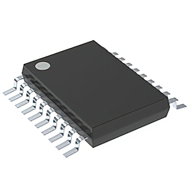
IC FLASH 8MBIT SPI 100MHZ 8SOIC
- In stock 866

AT25DF081A-SH-T Model Information
Basic Information
- Manufacturer: Renesas Electronics Corporation
- Product Family: Serial Flash Memory
- Device Density: 8-megabit (1MB)
- Interface: SPI (Serial Peripheral Interface)
- Operating Voltage: 2.7V to 3.6V
- Maximum Frequency: 100 MHz (RapidS Operation), 85 MHz (SPI Operation)
- Temperature Range: Industrial (-40°C to +85°C)
Package Information
- Package Type: 8-lead, 0.208" wide SOIC (EIAJ)
- Lead Finish: NiPdAu (Lead-free/Halide-free/RoHS Compliant)
- Package Drawing: 8S2
Features
- High-Speed Operation: Supports RapidS™ operation up to 100 MHz and SPI operation up to 85 MHz.
- Flexible Erase Architecture: Uniform 4-Kbyte, 32-Kbyte, and 64-Kbyte block erase options, as well as full chip erase.
- Individual Sector Protection: 16 sectors of 64-Kbytes each with hardware-controlled locking via the WP pin.
- Sector Lockdown: Permanently lock down any combination of 64-Kbyte sectors to make them read-only.
- OTP Security Register: 128-byte programmable OTP security register for unique device serialization, ESN storage, and locked key storage.
- Fast Program and Erase Times:Page Program (256 Bytes): 1.0 ms typical4-Kbyte Block Erase: 50 ms typical32-Kbyte Block Erase: 250 ms typical64-Kbyte Block Erase: 400 ms typical
- Low Power Dissipation:Active Read Current: 5 mA typical at 20 MHzDeep Power-Down Current: 5 µA typical
- Endurance: 100,000 program/erase cycles
- Data Retention: 20 years
- Compliance: Full industrial temperature range, RoHS compliant
Ordering Information
- Ordering Code: AT25DF081A-SH-T
- Shipping Carrier Option: Tape and reel
- Package Type: 8-lead, 0.208" wide SOIC (EIAJ)
- Lead Finish: NiPdAu
- Operating Voltage: 2.7V to 3.6V
- Maximum Frequency: 100 MHz (RapidS Operation), 85 MHz (SPI Operation)
- Temperature Range: Industrial (-40°C to +85°C)
Pin Descriptions
- CS (Chip Select): Asserting the CS pin selects the device. When deasserted, the device is deselected and placed in standby mode.
- SCK (Serial Clock): Provides the clock signal for data transfer.
- SI (Serial Input): Used to shift data into the device, including command and address sequences.
- SO (Serial Output): Used to shift data out from the device.
- WP (Write Protect): Controls hardware locking of protected sectors. Internally pulled high; can be left floating but should be externally connected to VCC if hardware protection is used.
- HOLD: Temporarily pauses serial communication without deselecting or resetting the device. Internally pulled high; can be left floating but should be externally connected to VCC if the Hold function is used.
Memory Organization
- Total Capacity: 8-megabit (1MB)
- Block Sizes:4-Kbyte blocks32-Kbyte blocks64-Kbyte blocks
- Sectors: 16 sectors of 64-Kbytes each
Commands and Operations
- Read Commands: Read Array (1Bh, 0Bh, 03h), Dual-Output Read Array (3Bh)
- Program and Erase Commands: Byte/Page Program (02h), Dual-Input Byte/Page Program (A2h), Block Erase (20h, 52h, D8h), Chip Erase (60h, C7h)
- Protection Commands: Write Enable (06h), Write Disable (04h), Protect Sector (36h), Unprotect Sector (39h), Global Protect/Unprotect, Sector Lockdown (33h), Freeze Sector Lockdown State (34h)
- Security Commands: Program OTP Security Register (9Bh), Read OTP Security Register (77h)
- Status Register Commands: Read Status Register (05h), Write Status Register Byte 1 (01h), Write Status Register Byte 2 (31h)
- Miscellaneous Commands: Reset (F0h), Read Manufacturer and Device ID (9Fh), Deep Power-Down (B9h), Resume from Deep Power-Down (ABh)
Electrical Specifications
- Absolute Maximum Ratings:Operating Temperature: -55°C to +125°CStorage Temperature: -65°C to +150°CInput Voltage: -0.6V to +4.1VOutput Voltage: -0.6V to VCC + 0.5V
- DC Characteristics:Standby Current (ISB): 25 µA to 50 µADeep Power-Down Current (IDPD): 5 µA to 10 µAActive Current (ICC1): 17 mA to 20 mA at 100 MHzActive Current (ICC2): 10 mA to 15 mA during program operationActive Current (ICC3): 12 mA to 18 mA during erase operation
- AC Characteristics:Maximum Clock Frequency: 100 MHz (RapidS), 85 MHz (SPI)Clock High Time (tCLKH): 4.3 nsClock Low Time (tCLKL): 4.3 nsData In Setup Time (tDS): 2 nsData In Hold Time (tDH): 1 nsOutput Valid Time (tV): 5 nsOutput Hold Time (tOH): 2 ns
Packaging Dimensions (8S2 - EIAJ SOIC)
- Body Size: 7.70 mm to 8.26 mm (width)
- Lead Length: 5.18 mm to 5.40 mm
- Lead Width: 1.27 mm (Basic Size)
- Lead Thickness: 0.35 mm to 0.48 mm
Revision History
- 8715F (2/2022): Changed company logo to Renesas.
- 8715E (11/2017): Added patent information.
- 8715D (8/2017): Updated corporate address.
- 8715C (1/2013): Update to Adesto logos, abbreviated title to SPI.
- 8715B (8/2010): Changed tRDPD Max from 10 to 30 in AC Parameters.
- 8715A (6/2010): Initial document release.
Purchase
No need to register to order from JMBom Electronics, but signing in lets you track your order like a pro. Give it a try for a smoother shopping ride.
Means
Easy peasy! Pay your way with PayPal, Credit Card, or wire transfer in USD. We've got you covered.
RFQ(Request for Quotations)
Get the freshest prices and stock updates by asking for a quote! Our sales team will shoot you an email within a day. It's that simple.
IMPORTANT NOTICE
1. Look out for your order details in your inbox! (If it's missing, check the spam folder just in case.)
2. Our sales manager will double-check the order and keep you posted on any price or stock changes. No worries, we've got you covered.

Shipping Rate
We ship orders once a day around 5 p.m., except Sunday. Once shipped, the estimated delivery time depends on the courier company you choose, usually 5-7 working days.

Shipping Methods
We provide DHL, FedEx, UPS, EMS, SF Express, and Registered Air Mail international shipping.


Payment
You can pay the orders on the website directly or pay by wire transfer offline. We support: Paypal、VISA、Credit Card.


Adesto Technologies