




 All Products

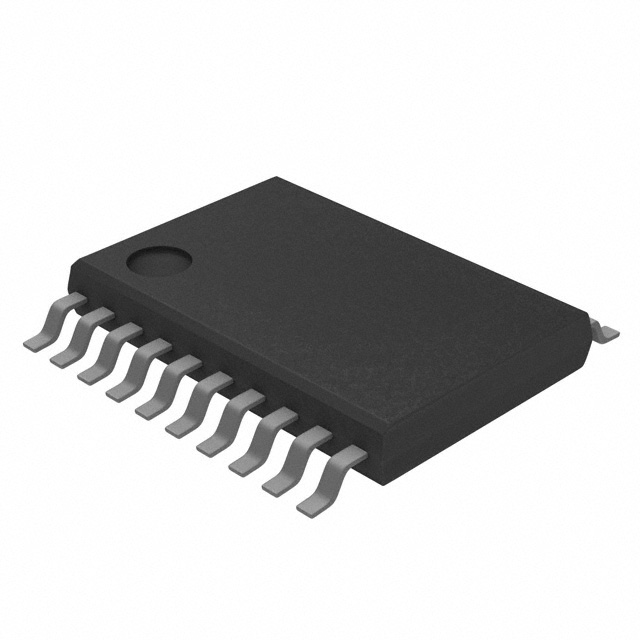
Texas Instruments(TI) M38510/34601BSA


- Part Number:
M38510/34601BSA
- Manufacturer:
- Category:
- RoHs:
 RoHS Compliant
- Datasheet:
 M38510/34601BSA_Datesheet
- Description:
OCTAL TRANSPARENT D-TYPE LATCHES
- In stock 0


M38510/34601BSA Military-Grade Octal Transparent D-Type Latch - Comprehensive Datasheet Summary
1. General Overview
The M38510/34601BSA is a military-qualified, high-reliability version of the SN54F373 octal transparent D-type latch with 3-state outputs. This device is manufactured in accordance with MIL-PRF-38535, the U.S. Department of Defense standard for integrated circuits.
Key Features:
- Eight Transparent D-Type Latches: Single package contains 8 latches for efficient board space utilization
- 3-State Bus-Driving Outputs: True outputs capable of driving high-capacitance or low-impedance loads
- Full Parallel Access: All eight latches can be loaded simultaneously
- Buffered Control Inputs: Latch Enable (LE) and Output Enable (OE) inputs are buffered for high drive capability
- Military Grade: Qualified to MIL-PRF-38535 Class B or QML (Qualified Manufacturers List) standards
- Wide Temperature Range: -55°C to +125°C operation
- Ceramic Flat Pack (CFP): Hermetic, high-reliability packaging for harsh environments
- High Reliability: Designed for aerospace, defense, and other mission-critical applications
2. Device Nomenclature and Ordering Information
Part Number Breakdown:
- M38510: Base specification for microcircuits (MIL-PRF-38535)
- 34601: Specific device identification number (SN54F373 equivalent)
- B: Military temperature range (-55°C to +125°C)
- S: Package type (CFP - Ceramic Flat Pack)
- A: Revision/version identifier
Ordering Information:
TableCopy
| Part Number | Status | Package | Military Standard | Temperature | Notes |
|---|---|---|---|---|---|
| M38510/34601BSA | ACTIVE | CFP (W) | MIL-PRF-38535 | -55°C to +125°C | Standard MIL-STD-883 processing |
| JM38510/34601BSA | ACTIVE | CFP (W) | MIL-PRF-38535 | -55°C to +125°C | JAN (Joint Army-Navy) designation |
| SNJ54F373W | ACTIVE | CFP (W) | MIL-PRF-38535 | -55°C to +125°C | TI commercial designation |
| 5962-9758901QSA | ACTIVE | CFP (W) | SMD (Standard Microcircuit Drawing) | -55°C to +125°C | SMD for procurement |
Additional Qualified Versions:
- 5962-9758901Q2A: LCCC package (FK) - Ceramic Chip Carrier
- 5962-9758901QRA: CDIP package (J) - Ceramic Dual Inline Package
- JM38510/34601B2A: LCCC package (FK)
- JM38510/34601BRA: CDIP package (J)
3. Pin Configuration
20-Pin Ceramic Flat Pack (CFP/W Package) - Top View:
Copy
       ┌───────────────────────┐
    5Q │1                    20│ VCC
     5D │2                    19│ 8Q
    VCC │3                    18│ 8D
     6Q │4                    17│ 7D
     6D │5                    16│ 7Q
    GND │6                    15│ LE
     1Q │7                    14│ GND
     1D │8                    13│ 4D
    OE │9                    12│ 4Q
   GND │10                   11│ 3D
       └───────────────────────┘
Pin Descriptions:
TableCopy
| Pin | Name | Type | Function |
|---|---|---|---|
| 1 | 5Q | Output | Data output for latch 5 |
| 2 | 5D | Input | Data input for latch 5 |
| 3 | VCC | Power | Supply voltage (+5V) |
| 4 | 6Q | Output | Data output for latch 6 |
| 5 | 6D | Input | Data input for latch 6 |
| 6 | GND | Power | Ground |
| 7 | 1Q | Output | Data output for latch 1 |
| 8 | 1D | Input | Data input for latch 1 |
| 9 | OE | Input | Output Enable (active low) - 3-state control |
| 10 | GND | Power | Ground |
| 11 | 3D | Input | Data input for latch 3 |
| 12 | 4Q | Output | Data output for latch 4 |
| 13 | 4D | Input | Data input for latch 4 |
| 14 | GND | Power | Ground |
| 15 | LE | Input | Latch Enable (active high) - transparent when high |
| 16 | 7Q | Output | Data output for latch 7 |
| 17 | 7D | Input | Data input for latch 7 |
| 18 | 8D | Input | Data input for latch 8 |
| 19 | 8Q | Output | Data output for latch 8 |
| 20 | VCC | Power | Supply voltage (+5V) Note: This pinout differs from the commercial SN74F373 DB/DW/N packages. The CFP package has a unique pin configuration optimized for military applications. |
4. Functional Description
Operation Modes:
TableCopy
| LE | OE | D Input | Q Output | Mode |
|---|---|---|---|---|
| H | L | H | H | Transparent |
| H | L | L | L | Transparent |
| L | L | X | Q0 | Latched (hold) |
| X | H | X | Z | 3-State (disabled) |
- Transparent Mode: When LE is HIGH, Q outputs follow D inputs
- Latched Mode: When LE goes LOW, Q outputs hold the data present at the falling edge
- 3-State Mode: When OE is HIGH, all outputs enter high-impedance state (Hi-Z)
- OE does not affect internal operation: Data can be latched or changed while outputs are disabled
Logic Diagram:
Each of the 8 latches consists of:
- Data Input Buffer: Schmitt-trigger input for noise immunity
- Latch Enable Gate: Controls transparency/latch function
- Latch Storage Element: Cross-coupled inverters store data
- 3-State Output Buffer: Controlled by OE input, drives external loads
5. Absolute Maximum Ratings
TableCopy
| Parameter | Symbol | Value | Units |
|---|---|---|---|
| Supply Voltage Range | VCC | -0.5 to +7.0 | V |
| Input Voltage Range | VI | -1.2 to +7.0 | V |
| Input Current Range | II | -30 to +5 | mA |
| Output Voltage Range (High State) | VO | -0.5 to VCC | V |
| Output Voltage Range (Disabled/Power-OFF) | VO | -0.5 to +5.5 | V |
| Low-Level Output Current | IOL | 40 | mA |
| Operating Temperature Range | TA | -55 to +125 | °C |
| Storage Temperature Range | Tstg | -65 to +150 | °C |
| ESD Rating (HBM) | ESD | >2000 | V Note: Stresses beyond these ratings may cause permanent damage. Functional operation should be within recommended operating conditions. |
6. Recommended Operating Conditions
TableCopy
| Parameter | Symbol | Min | Nom | Max | Units |
|---|---|---|---|---|---|
| Supply Voltage | VCC | 4.5 | 5.0 | 5.5 | V |
| High-Level Input Voltage | VIH | 2.0 | - | VCC | V |
| Low-Level Input Voltage | VIL | -0.5 | - | 0.8 | V |
| High-Level Output Current | IOH | - | - | -3 | mA |
| Low-Level Output Current | IOL | - | - | 20 | mA |
| Operating Temperature Range | TA | -55 | - | +125 | °C |
7. Electrical Characteristics (VCC = 4.5V to 5.5V, TA = -55°C to +125°C)
DC Characteristics:
TableCopy
| Parameter | Test Conditions | Min | Max | Units |
|---|---|---|---|---|
| Input Clamp Voltage (VIK) | VCC=4.5V, II=-18mA | - | -1.2 | V |
| High-Level Output Voltage (VOH) | VCC=4.5V, IOH=-1mA | 2.5 | - | V |
| High-Level Output Voltage (VOH) | VCC=4.5V, IOH=-3mA | 2.4 | - | V |
| Low-Level Output Voltage (VOL) | VCC=4.5V, IOL=20mA | - | 0.5 | V |
| Input Current (II) | VCC=5.5V, VI=7V | - | 0.1 | mA |
| High-Level Input Current (IIH) | VCC=5.5V, VI=2.7V | - | 20 | μA |
| Low-Level Input Current (IIL) | VCC=5.5V, VI=0.5V | - | -0.6 | mA |
| Short-Circuit Output Current (IOS) | VCC=5.5V, VO=0 | -60 | -150 | mA |
| Quiescent Supply Current (ICCZ) | VCC=5.5V, OE=4.5V, other inputs=GND | - | 55 | mA Note: Not more than one output should be shorted at a time, and duration should not exceed 1 second. |
8. Timing Requirements and Switching Characteristics
Timing Requirements:
TableCopy
| Parameter | Symbol | Min | Max | Units |
|---|---|---|---|---|
| LE Pulse Duration (High) | tw | 6 | - | ns |
| Data Setup Time (before LE↓) | tsu | 2 | - | ns |
| Data Hold Time (after LE↓) | th | 3 | - | ns |
Switching Characteristics (CL = 50pF, RL = 500Ω):
TableCopy
| Parameter | From (Input) | To (Output) | Min | Max | Units |
|---|---|---|---|---|---|
| Propagation Delay (Low-to-High) | D | Q | 2.2 | 8.5 | ns |
| Propagation Delay (High-to-Low) | D | Q | 1.2 | 7.0 | ns |
| Propagation Delay (Low-to-High) | LE | Q | 4.2 | 15.0 | ns |
| Propagation Delay (High-to-Low) | LE | Q | 2.2 | 8.5 | ns |
| Output Enable Time (High-to-Z) | OE | Q | 1.2 | 13.5 | ns |
| Output Disable Time (Z-to-Low) | OE | Q | 1.2 | 10.0 | ns |
| Output Disable Time (Z-to-High) | OE | Q | 1.2 | 7.5 | ns |
| Output Enable Time (Low-to-Z) | OE | Q | 1.2 | 7.0 | ns |
9. Military Standard Compliance
QML Qualification:
- QML Class Q: Qualified to MIL-PRF-38535, Appendix Q (highest reliability)
- QML Class V: Space-level qualification available (MIL-PRF-38535, Appendix V)
- SMD Number: 5962-9758901QSA
Processing and Testing:
- Wafer Lot Acceptance: Per MIL-PRF-38535
- Element Evaluation: 100% screening including temperature cycling, burn-in, and electrical testing
- Group A Testing: Electrical parameters tested at +25°C, +125°C, and -55°C
- Group B/C Testing: Periodic reliability and quality conformance testing
- Traceability: Complete device traceability to wafer lot and assembly date
- Radiation Hardness: Available in radiation-hardened versions (contact TI for details)
Quality Conformance:
- MIL-STD-883: All devices tested per Method 5004 (Class B) and Method 5005 (Class S)
- ESD Sensitivity: Class 2 (2000V to 3999V HBM)
- Moisture Sensitivity: Not applicable (hermetic package)
- Outgassing: Meets NASA requirements for space applications
10. Package Information
20-Pin Ceramic Flat Pack (CFP) - W Package:
- Package Type: CFP (Ceramic Flat Pack), also known as "Flat Pack" or "Wing"
- Body Dimensions:Width: 0.4" (10.16mm) typicalLength: 0.5" (12.7mm) typicalHeight: 0.1" (2.54mm) maximum
- Lead Pitch: 0.1" (2.54mm)
- Lead Count: 20 leads
- Materials:Body: Alumina ceramic (hermetic)Leads: Kovar alloy, gold-platedLid: Ceramic or metal, seam-sealed
- Weight: Approximately 1.5 grams
- Mounting: Through-hole or surface mount (with lead forming)
Hermeticity:
- Seal Test: Per MIL-STD-883, Method 1014
- Leak Rate: ≤ 5×10⁻⁸ atm·cc/s (fine leak)
- Moisture Content: ≤ 5000 ppm internal water vapor
11. Application Information
Typical Applications:
- Military Bus Interface: 3-state capability ideal for MIL-STD-1553 or other military bus systems
- Aerospace Data Buffer: High-reliability data storage in avionics systems
- Radiation-Hardened Systems: Space-qualified versions for satellite applications
- Weapon Systems: Fire control, guidance, and communication systems
- Ground Support Equipment: Test equipment requiring MIL-STD compliance
Design Considerations:
Power Supply Decoupling:
- Use 0.1μF ceramic capacitor on each VCC pin (pins 3 and 20)
- Add 10μF tantalum capacitor for bulk decoupling within 0.5" of device
- Use separate power planes for analog and digital if applicable
- Thermal Management:
- With thermal resistance θJA ≈ 40-50°C/W (CFP), ensure adequate airflow
- Derate maximum power dissipation above 85°C ambient
- Use thermal vias under package for enhanced heat dissipation
- Layout Guidelines:
- Keep trace lengths short for LE and OE control signals
- Use ground plane for improved noise immunity
- Match trace lengths for D0-D7 if using in synchronous applications
- Avoid routing high-speed signals under package
- Unused Pins:
- Tie unused data inputs to VCC or GND
- Do not float unused outputs (leave unconnected if 3-state is active)
- OE should be tied to GND if always enabled
12. Reliability and Failure Rate
Predicted Reliability (per MIL-HDBK-217):
- Ground Benign: 0.002 failures/10⁶ hours
- Airborne Inhabited Cargo: 0.008 failures/10⁶ hours
- Airborne Uninhabited Fighter: 0.02 failures/10⁶ hours
- Space: 0.05 failures/10⁶ hours (GEO), 0.1 failures/10⁶ hours (LEO)
Failure Analysis:
- Failure Mode: Typically open/short on I/O or power pins
- Acceleration Factors: AF = 2.0 per 10°C temperature increase
- Screening Effectiveness: 95% defect removal with Class S processing
13. Export Control and ITAR
Export Classification:
- ECCN: 3A001.a.2.c (if not space-qualified)
- USML Category: XI(b) if space-qualified
- ITAR Restrictions: May require State Department export license
- Note: This device may be subject to International Traffic in Arms Regulations (ITAR) or Export Administration Regulations (EAR). Contact TI or appropriate government agency for export licensing requirements.
14. Documentation and Support
Primary Documentation:
- SMD: 5962-9758901 (latest revision)
- Standard Microcircuit Drawing: Available from DSCC (Defense Supply Center Columbus)
- Test Specification: MIL-STD-883
- Qualification Report: Available under NDA
Related Standards:
- MIL-PRF-38535: Integrated Circuits (Microcircuits) Manufacturing
- MIL-STD-883: Test Methods and Procedures for Microelectronics
- QML-38535: Qualified Manufacturers List Program
Purchase
No need to register to order from JMBom Electronics, but signing in lets you track your order like a pro. Give it a try for a smoother shopping ride.
Means
Easy peasy! Pay your way with PayPal, Credit Card, or wire transfer in USD. We've got you covered.
RFQ(Request for Quotations)
Get the freshest prices and stock updates by asking for a quote! Our sales team will shoot you an email within a day. It's that simple.
IMPORTANT NOTICE
1. Look out for your order details in your inbox! (If it's missing, check the spam folder just in case.)
2. Our sales manager will double-check the order and keep you posted on any price or stock changes. No worries, we've got you covered.

Shipping Rate
We ship orders once a day around 5 p.m., except Sunday. Once shipped, the estimated delivery time depends on the courier company you choose, usually 5-7 working days.

Shipping Methods
We provide DHL, FedEx, UPS, EMS, SF Express, and Registered Air Mail international shipping.


Payment
You can pay the orders on the website directly or pay by wire transfer offline. We support: Paypal、VISA、Credit Card.





Texas Instruments(TI)
Texas Instruments(TI)
Texas Instruments(TI)
Texas Instruments(TI)
Texas Instruments(TI)
Texas Instruments(TI)
Texas Instruments(TI)
Texas Instruments(TI)
Texas Instruments(TI)
Texas Instruments(TI)
Texas Instruments(TI)
Texas Instruments(TI)