
Texas Instruments(TI) TPS22950CQDDCRQ1


- Part Number:
TPS22950CQDDCRQ1
- Manufacturer:
- Category:
- RoHs:
 RoHS Compliant
 - Datasheet:
 TPS22950CQDDCRQ1_Datesheet
 - Description:
AUTOMOTIVE 5.5-V, 2.7-A, 34-M LO
- In stock 892

TPS22950CQDDCRQ1 Complete Supplementary Datasheet Summary
1. Basic Identification
- Full Part Number: TPS22950CQDDCRQ1
- Device Family: TPS22950‑Q1 Automotive Grade Load Switch
- Status: Active (Production)
- Qualification: AEC‑Q100 Grade 1
- RoHS Compliance: Yes
- Operating Temperature: −40 °C to 125 °C
- Top Marking: 950Q
- Certification: UL 2367 (File No. E169910, 66 mA – 2.46 A)
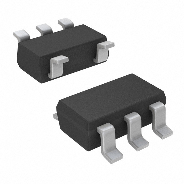
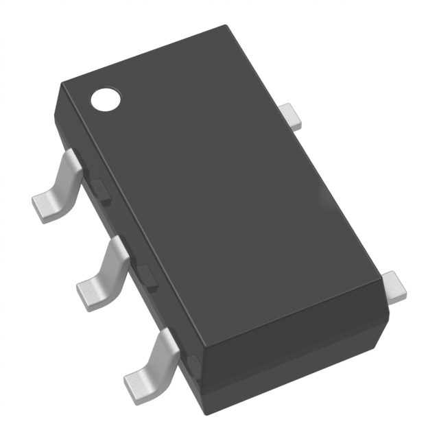
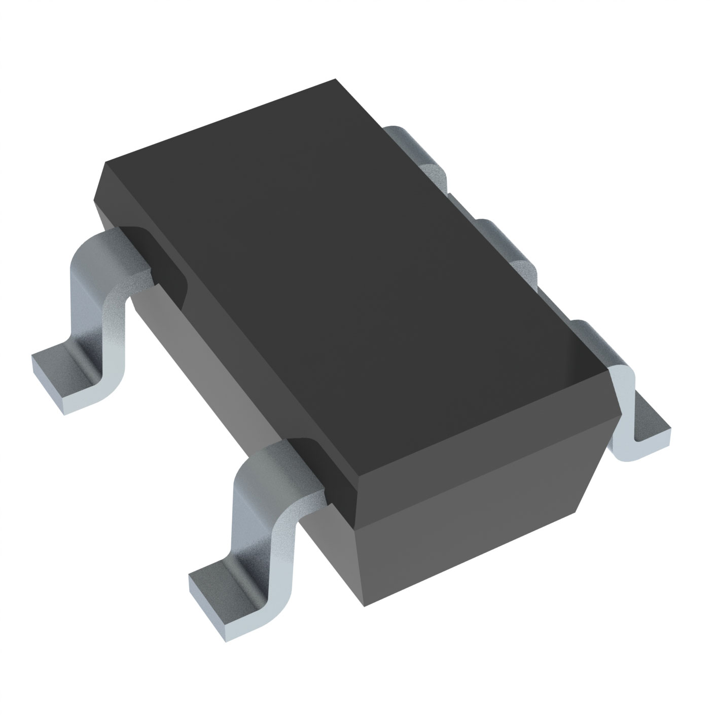
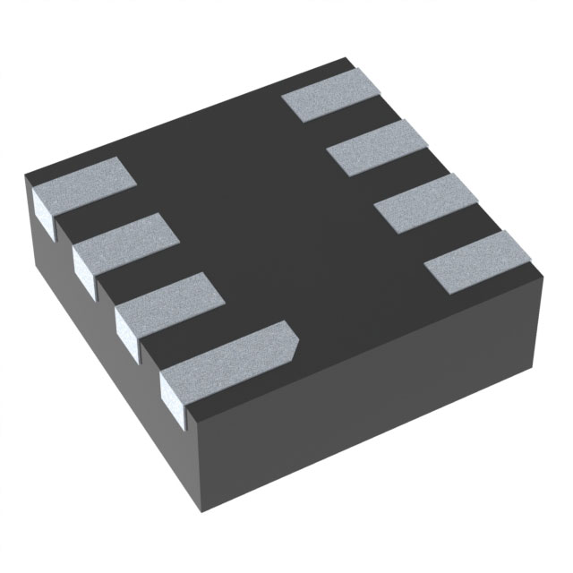
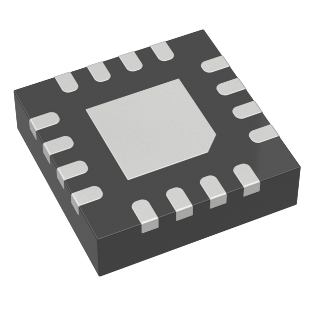
2. Package & Mechanical Data
- Package Type: SOT‑23‑THIN (DDC)
- Pin Count: 6 pins
- Nominal Body Size: 2.90 mm × 2.80 mm
- Max Height: 1.1 mm
- Thermal Resistance (RθJA): 104.8 °C/W
- MSL Rating: Level 1, 260 °C peak reflow, unlimited floor life
- Lead Finish: SN
3. Packaging & Tape-and-Reel Specifications
3.1 Packaging Configuration
- Standard Pack Quantity (SPQ): 3000 units per reel
- Carrier: Large Tape and Reel (LARGE T&R)
3.2 Reel Dimensions (Nominal)
- Reel Diameter: 180.0 mm
- Reel Width (W1): 8.4 mm
- Carrier Tape Width (W): 8.0 mm
- Cavity Pitch (P1): 4.0 mm
- Cavity Length (A0): 3.2 mm
- Cavity Width (B0): 3.2 mm
- Cavity Height (K0): 1.4 mm
- Pin 1 Quadrant: Q3
3.3 Reel Box Dimensions (Nominal)
- Length: 210.0 mm
- Width: 185.0 mm
- Height: 35.0 mm
4. Absolute Maximum Ratings
- VIN, VOUT, VON, VFLT: −0.3 V to 6 V
- Continuous Output Current (IMAX): 2.7 A
- Pulsed Output Current (IMAX,PLS): 4.1 A (TJ = 85 °C, 2% duty cycle)
- Storage Temperature (TSTG): −65 °C to 150 °C
- Lead Soldering Temp (10 s): 300 °C
5. Recommended Operating Conditions
- Input Voltage (VIN): 1.8 V – 5.5 V
- Output Voltage (VOUT): 0 V – 5.5 V
- Current Limit (ILIM): 0.05 A – 3.5 A (typ)
- Ambient Temp (TA): −40 °C – 125 °C
- Junction Temp (TJ): −40 °C – 150 °C
- ON Pin High (VIH): 1 V – 5.5 V
- ON Pin Low (VIL): 0 V – 0.35 V
6. Key Electrical Characteristics
6.1 Supply Current
- Quiescent Current (IQ): 40 µA typ (ON, VIN = 5 V)
- Shutdown Current (ISD): 0.2 µA typ (OFF, 25 °C)
6.2 ON‑Resistance (RON)
- VIN = 5 V: 34 mΩ typ, 41 mΩ max
- VIN = 3.3 V: 41 mΩ typ, 51 mΩ max
- VIN = 1.8 V: 65 mΩ typ, 90 mΩ max
6.3 Current Limit (ILIM)
- Adjustable via external resistor to GND: ILIM = 1.18 × (RILIM)⁻¹·⁰⁷²
- Response time (tLIM): 5 µs typ
6.4 Reverse Current Blocking (RCB)
- Activation threshold: 44 mV typ (VOUT > VIN)
- Release threshold: 16 mV typ
- Response time (tRCB): 3 µs typ
6.5 Fault Indicator (FLT)
- Open‑drain, low in fault
- VOL, FLT: 0.1 V max at IFLT = 1 mA
6.6 Quick Output Discharge (QOD)
- 130 Ω typ (VIN = 5 V, OFF state)
6.7 Thermal Shutdown (TSD)
- Trigger: 170 °C (rising)
- Release: 150 °C (falling, hysteresis)
7. Switching Characteristics (Typical, 25 °C)
- tON (Turn‑on Time):
- tR (Rise Time):
- tOFF (Turn‑off Time):
- tFALL (Fall Time): ~118–130 µs
- Output Delay (tD): 415 µs (all VIN)
8. Pin Configuration (6‑Pin DDC SOT, Top View)
表格
| Pin No. | Name | Type | Description |
|---|---|---|---|
| 1 | ON | Input | Active‑high enable; do not float |
| 2 | VIN | Power | Supply input |
| 3 | GND | Ground | Device ground |
| 4 | ILIM | I/O | Current‑limit adjust (resistor to GND) |
| 5 | VOUT | Power | Switch output |
| 6 | FLT | Output | Open‑drain fault signal |
9. Core Features
- Adjustable output current limit (0.05 A – 3.5 A)
- Always‑ON true reverse current blocking (RCB)
- Thermal shutdown with hysteresis
- Open‑drain fault indication (FLT)
- Smart ON‑pin pulldown (prevents floating)
- Slow turn‑on to minimize inrush current
- Quick output discharge (QOD) when disabled
- Ultra‑low quiescent and shutdown current
10. Typical Applications
- Automotive infotainment & cluster head units
- Automotive dashboard displays
- ADAS surround‑view ECUs
- Body control modules & gateways
11. Reliability & Handling
- ESD Rating: HBM ±2000 V; CDM ±500 V
- ESD Caution: Use proper ESD protection during handling
- Junction Temperature: −40 °C to 150 °C
12. Layout Guidelines
- Place RILIM close to ILIM pin and minimize ground loop
- Input/output capacitors near device to reduce parasitics
- Wide copper traces for VIN, VOUT, GND to improve thermal dissipation
- Minimize AC current loop area to reduce noise
Purchase
No need to register to order from JMBom Electronics, but signing in lets you track your order like a pro. Give it a try for a smoother shopping ride.
Means
Easy peasy! Pay your way with PayPal, Credit Card, or wire transfer in USD. We've got you covered.
RFQ(Request for Quotations)
Get the freshest prices and stock updates by asking for a quote! Our sales team will shoot you an email within a day. It's that simple.
IMPORTANT NOTICE
1. Look out for your order details in your inbox! (If it's missing, check the spam folder just in case.)
2. Our sales manager will double-check the order and keep you posted on any price or stock changes. No worries, we've got you covered.

Shipping Rate
We ship orders once a day around 5 p.m., except Sunday. Once shipped, the estimated delivery time depends on the courier company you choose, usually 5-7 working days.

Shipping Methods
We provide DHL, FedEx, UPS, EMS, SF Express, and Registered Air Mail international shipping.


Payment
You can pay the orders on the website directly or pay by wire transfer offline. We support: Paypal、VISA、Credit Card.


Texas Instruments(TI)
Texas Instruments(TI)
Texas Instruments(TI)
Texas Instruments(TI)
Texas Instruments(TI)
Texas Instruments(TI)
Texas Instruments(TI)
Texas Instruments(TI)
Texas Instruments(TI)
Texas Instruments(TI)
Texas Instruments(TI)

Texas Instruments(TI)