


TPS7A11 LDO Regulator for Low-Voltage Battery Applications
Catalog
What is the TPS7A11 Regulator?Functional Block Diagram & Key Performance FeaturesKey Features and Operation Modes of TPS7A11Package and Pinout InformationDRV Package Pin DetailsYKA (5-Pin DSBGA) Package PinoutTPS7A11 Electrical SpecificationsTypical Applications of the TPS7A11 RegulatorFrequently Ask QuestionsRelated ArticlesToday’s portable devices often rely on battery power, making voltage regulators essential components. As demand grows for ultra-low voltage operation in sensitive electronics, Low Dropout (LDO) regulators have become increasingly important. These regulators are capable of maintaining output voltage even when the input is only slightly higher—typically between 200mV and 500mV. Compact and efficient power solutions are especially critical for portable systems, where low input and output voltages are common. The TPS7A11 is one such LDO regulator designed to meet these requirements.
TPS7A11 Low Dropout Voltage Regulator
What is the TPS7A11 Regulator?
The TPS7A11 is an ultra-low dropout voltage regulator with a compact form factor and very low quiescent current. It can maintain regulation with an input voltage just 140mV above the output.
Thanks to its dedicated VBIAS rail, which supplies power to the internal circuitry, the TPS7A11 can operate effectively with extremely low input voltages. These features make it a great choice for battery-operated and energy-sensitive applications.
Functional Block Diagram & Key Performance Features
Block Diagram
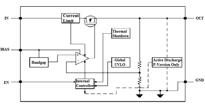
Fast Transient Performance
Thanks to its high input impedance and low output impedance, the TPS7A11 offers rapid response to changes in input voltage or output load.
This quick reaction helps maintain stable output during sudden load or supply variations.
Additionally, these design characteristics contribute to the device’s high power supply rejection ratio (PSRR) and a low internal noise level. The TPS7A11 demonstrates strong performance in both load and line transient conditions.
Integrated Undervoltage Lockout (UVLO) Protection
The TPS7A11 includes two built-in undervoltage lockout (UVLO) circuits—one on the BIAS pin and the other on the IN pin. These circuits ensure that the device does not power on until both the BIAS and IN voltages exceed their respective thresholds.
Internally, these UVLO signals are fed into an AND logic gate. This means the regulator will remain off unless both input voltages are above their minimum required levels, adding an extra layer of startup protection.
Key Features and Operation Modes of TPS7A11
Active Output Discharge
To safely discharge the output when the device is turned off, the TPS7A11 includes an internal pull-down MOSFET. This MOSFET connects a 120Ω resistor to ground when the device is disabled. The discharge function activates automatically when the EN (enable) pin is low or when the device enters thermal shutdown.
Built-In Foldback Current Limiting
An internal foldback current limit mechanism protects the regulator during overcurrent conditions or in the event of an output short circuit. This feature helps reduce power dissipation and enhances device reliability under fault conditions.
Thermal Shutdown Protection
If the junction temperature exceeds a safe threshold, the TPS7A11 automatically shuts down to prevent thermal damage. Once the temperature drops below this threshold, the built-in hysteresis ensures the device restarts safely without oscillation.
TPS7A11 Operating Modes
The regulator operates in three main modes:
- Normal Mode: Provides regulated output within specifications.
- Dropout Mode: Output voltage drops to approximately the input voltage minus the dropout voltage when the input is too low for full regulation.
- Shutdown Mode: The regulator is turned off completely, typically via the EN pin or thermal shutdown.
Application Circuit and External Components
Typical Application Circuit
Depending on the target application, external passive components are required for proper performance. These typically include capacitors at the input, output, and bias pins.
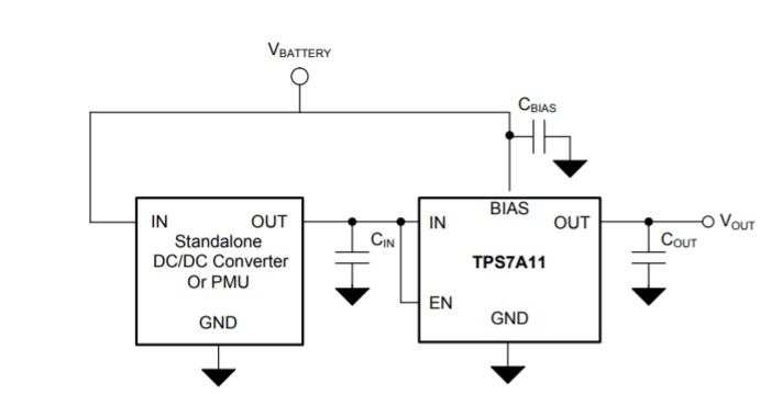
Circuit Diagram of TPS7A11
Recommended Capacitor Types
TPS7A11 is designed to work best with ceramic capacitors, particularly multilayer ceramic capacitors (MLCCs). Care should be taken with capacitor selection to ensure stability.
Input and Output Capacitor Guidelines
- Input Capacitor: Minimum 2.2 µF
- Output Capacitor: Minimum 2.2 µF, Maximum 22 µF
- Bias Capacitor: 0.1 µF recommended
Package and Pinout Information
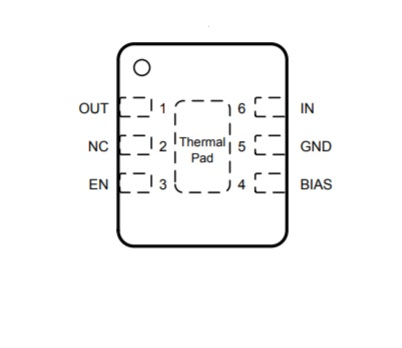
DRV package of TPS7A11
TPS7A11 is offered in two compact package options to suit space-constrained designs:
- 6-Pin WSON (DRV): 2.00 mm × 2.00 mm
- 5-Pin DSBGA (YKA): Ultra-small 0.74 mm × 1.09 mm
These options allow designers flexibility when integrating the LDO into miniature or portable systems.
DRV Package Pin Details
For optimal thermal performance, the exposed thermal pad on the DRV package should be connected to ground.
- Pin 1 (OUT): This is the regulated output pin. To ensure stability, connect a capacitor between OUT and ground. For improved transient response, place a ceramic capacitor as close as possible to this pin.
- Pin 2 (NC): This pin is not internally connected. It can be left floating or tied to ground to aid in thermal dissipation.
- Pin 3 (EN): Enable pin. Pulling this pin high turns the device on; pulling it low disables it. For automatic enable functionality, it can be tied to either the IN or BIAS pin—provided the IN voltage is above 0.9 V.
- Pin 4 (BIAS): Bias supply input. This pin enables the regulator to function with low input and output voltages. To achieve optimal performance, a capacitor should be placed from BIAS to ground.
- Pin 5 (GND): Ground connection.
- Pin 6 (IN): Input supply pin. A capacitor is recommended between this pin and ground for stability. It should be placed close to the IN pin.
YKA (5-Pin DSBGA) Package Pinout
The pin functionality for the YKA package is equivalent to the DRV version, with the following pin layout:
- A1: Input pin (IN)
- A3: Output pin (OUT)
- B2: Ground pin (GND)
- C1: Bias input (BIAS)
- C3: Enable pin (EN)
TPS7A11 Electrical Specifications
Key performance features and specs for TPS7A11 include:
- Supports ultra-low output voltages from 0.75 V to 3.3 V
- Available in two compact packages: DRV (WSON) and YKA (DSBGA)
- Low dropout voltage: DRV package: 140 mV at 500 mA YKA package: 110 mV at 500 mA
- Low quiescent current: 1.6 µA from VIN 6 µA from VBIAS
- Tight regulation accuracy of ±1.5% across load, line, and temperature
- High power supply rejection ratio (PSRR): 64 dB at 1 kHz
- Includes active output discharge for controlled shutdown behavior
- Available with fixed output voltage options from 0.5 V to 3 V
- VBIAS operating range: 1.7 V to 5.5 V
- Recommended junction temperature range: –40°C to +125°C
- Supports output voltages from 0.5 V to 3 V under full temperature range
- Requires a 0.1 µF bias capacitor for optimal operation
- Maximum ESR (Equivalent Series Resistance) for stability must be <250 mΩ under operating temperature
Typical Applications of the TPS7A11 Regulator
The TPS7A11 is widely used in low-voltage and compact electronic systems. Its common applications include:
- Powering the low-core voltage domains of modern microcontrollers and precision sensors
- Embedded in wearable devices like smartwatches and fitness trackers
- Utilized in wireless audio products such as headphones and earbuds
- Integrated into camera modules for portable electronics
- Found in medical wearables, smartphones, tablets, and solid-state storage devices
Alternative Option
A suitable alternative to the TPS7A11 is the TPS7A26, which also supports low-voltage operation.
Thanks to its ability to function with both low input and low output voltages, the TPS7A11 is an excellent choice for battery-operated, noise-sensitive portable electronics. While conventional LDOs may offer similar voltage support, they typically operate with lower efficiency.
The TPS7A11 overcomes this by using a separate bias rail, allowing it to regulate output at low input voltages while minimizing power loss across the device. More technical details and electrical characteristics can be found in the official datasheet from Texas Instruments.
Have you used the TPS7A11 in your design?
What capacitor values have you implemented in your circuit for input, output, and bias filtering?
Frequently Ask Questions
What is the function of a low dropout (LDO) voltage regulator?
A low dropout regulator (LDO) helps maintain a stable output voltage even when the input voltage is only slightly higher. It’s a cost-effective and straightforward solution for applications that don’t require high efficiency. LDOs are simple to implement, and their datasheet specifications are generally easy to interpret for most designs.
Why do voltage regulators fail?
Voltage regulators typically degrade over time due to age and regular wear. However, failures can also result from external factors, like a weak battery, poor grounding, or a malfunctioning alternator, all of which can shorten the regulator’s lifespan.
What is the dropout voltage in a switching regulator?
For a typical switching regulator, the dropout voltage — the point where the output can no longer stay regulated — usually falls between 1.5V and 2.2V. This value can vary depending on the load current and ambient temperature.
What does a low voltage regulator mean?
A low voltage regulator, specifically an LDO, is a type of linear regulator that can operate with a very small difference between input and output voltage. It provides a constant output voltage and is commonly used in electronics where space and simplicity are key.
What are the symptoms of a bad voltage regulator?
When a voltage regulator fails in a vehicle, electrical components may start to behave unpredictably or stop working altogether. This happens because the regulator can no longer ensure a steady flow of voltage to the system.
What are the drawbacks of using an LDO regulator?
LDOs can become inefficient if there’s a large gap between input and output voltage or if the current demand is high. This leads to increased heat dissipation, which can cause thermal issues or force the regulator into shutdown mode, especially in compact or poorly ventilated packages.
Related Articles
TLV3201AQDCKRQ1 Comparator: Pinout, Operation, and Typical Uses
OPT3007 Ultra-Thin Ambient Light Sensor Overview and Applications
TPS7A26 LDO Regulator: Functionality and Key Applications
Guide to Low Dropout (LDO) Regulators and How They Work
ESP32-S3 Development Board: Pinout Diagram, Key Features, Technical Specs
DS18B20 Waterproof Temperature Sensor: Overview, Operation, and Common Uses
BAT54A Schottky Diode: Pinout and Common Uses

Christopher Anderson
Christopher Anderson has a Ph.D. in electrical engineering, focusing on power electronics. He’s been a Senior member of the IEEE Power Electronics Society since 2021. Right now, he works with the KPR Institute of Engineering and Technology in the U.S. He also writes detailed, top-notch articles about power electronics for business-to-business electronics platforms.
Subscribe to JMBom Electronics !


