


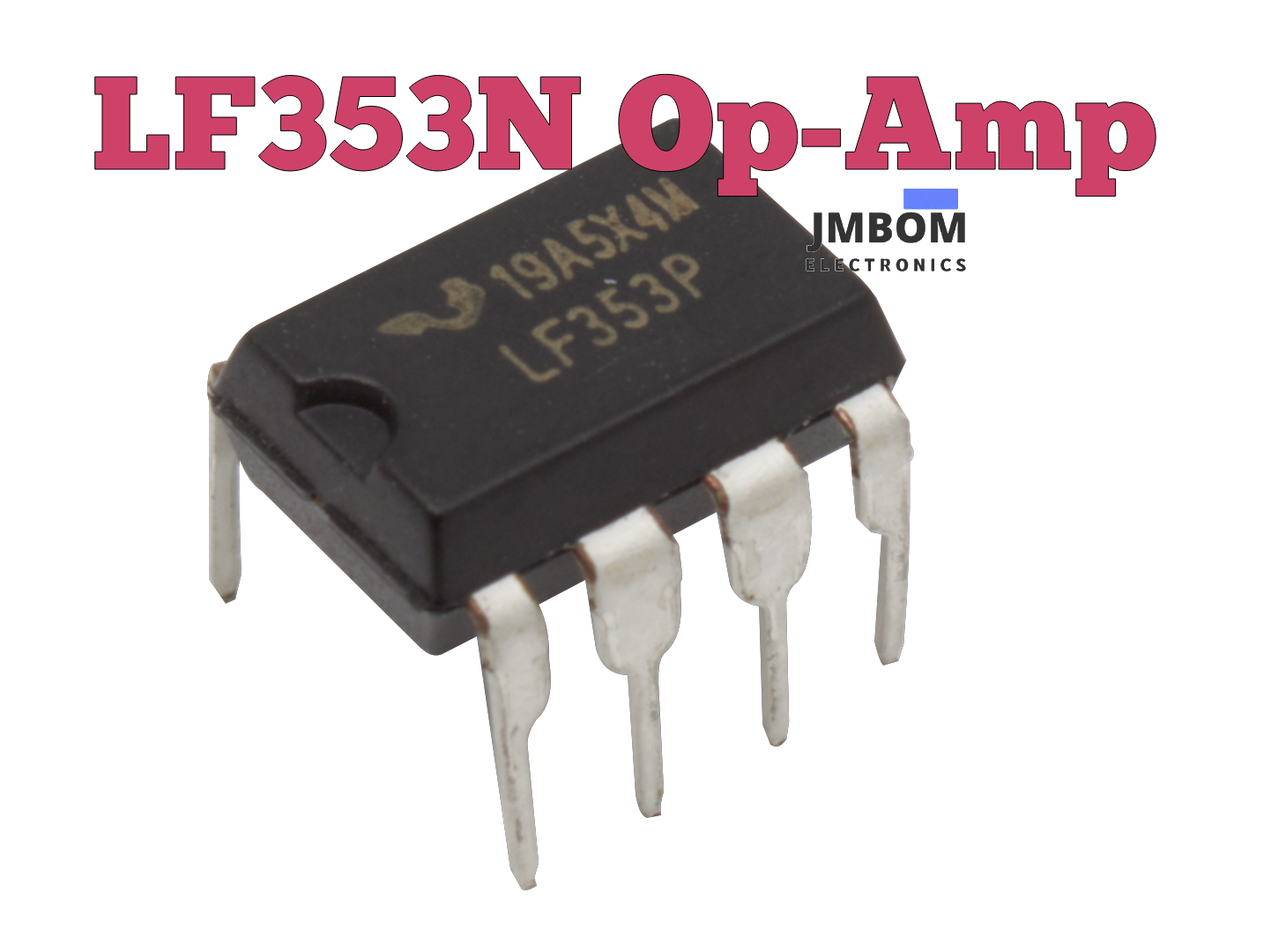
LF353N Op-Amp Explained: Pinout, Features, and How It Works
Catalog
What is the LF353N Op-Amp?LF353N JFET Dual Op-Amp: Features, Pinout, and Key ApplicationsPinout DiagramTechnical SpecificationsLF353N Electrical Characteristics, Usage Guide, and Equivalent OptionsHow to Use the LF353N: Circuit ExampleKey Setup Guidelines for 3-Way Crossover NetworkWhere to Use the LF353N Op-Amp: ApplicationsSummaryLF351 Equivalent ICs and Common Op-Amp Questions AnsweredRelated ArticlesBack in 1968, FAIRCHILD launched a compact, reliable, and energy-efficient multi-stage amplifier known as the operational amplifier, packaged as a monolithic IC. Later, Texas Instruments introduced the LF353N—a dual JFET-input op-amp known for its high input impedance, thanks to its JFET-based input stage. In this article, we’ll cover an overview of the LF353N op-amp, its pin layout, technical details, typical circuit usage, and key applications.
What is the LF353N Op-Amp?
The LF353N is a dual op-amp featuring JFET inputs and an internally calibrated offset voltage. These op-amps deliver high-speed performance while operating on low supply current, making them both efficient and cost-effective. With a high slew rate and wide gain-bandwidth product, they are ideal for applications requiring speed and precision. The matched high-voltage JFET input stage ensures minimal input bias and offset currents. The LF353N is also considered a performance-compatible upgrade over classic op-amps like the LM1558 and LM358.
LF353N JFET Dual Op-Amp: Features, Pinout, and Key Applications
The LF353N is a dual-input JFET operational amplifier developed by Texas Instruments. Its inputs are connected through high-voltage JFET transistors, which allow it to deliver low noise, low power consumption, and fast switching—ideal for audio applications, especially in systems powered by dual supplies.
Thanks to the JFET input stage, the LF353N offers high input impedance and a wide bandwidth of up to 4 MHz, along with a fast slew rate of 13 V/μs. These characteristics make it a strong choice for audio amplification and other analog signal processing tasks.
It also features low input noise and minimal input bias current, further enhancing its suitability for audio-focused designs. The op-amp is optimized for dual power supply operation up to ±18V. When operating with a single supply, the output swing is typically limited—dropping as low as 0.7V on the low end and topping out at about 1.5V on the high end. Because of this, the LF353N is most commonly found in analog or audio circuit designs. For digital circuit applications, a comparable part would be the Microchip MCP6002.
Pinout Diagram
The LF353N op-amp comes in an 8-pin IC package, available in both PDIP and SOIC formats. The pin configuration is shown below:
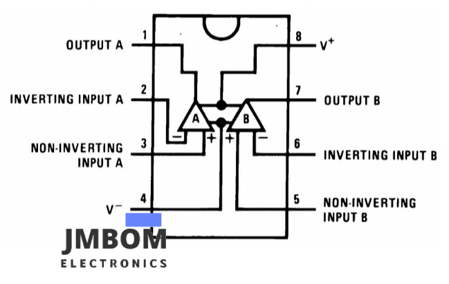
Pin Diagram of LF353N Op-Amp
Pin Description:
- Pin 1 (Output A): This is the output terminal of op-amp channel A.
- Pin 2 (Inverting Input A): This is the inverting input for op-amp A.
- Pin 3 (Non-Inverting Input A): This is the non-inverting input for op-amp A.
- Pin 4 (VEE/GND or V−): This pin is used for the negative power supply or ground connection.
- Pin 5 (Non-Inverting Input B): This is the non-inverting input for op-amp B.
- Pin 6 (Inverting Input B): This is the inverting input for op-amp B.
- Pin 7 (Output B): This is the output terminal of op-amp channel B.
- Pin 8 (VCC or V+): This pin connects to the positive supply voltage.
Technical Specifications
Below are the main technical specifications of the LF353N dual JFET-input operational amplifier:
Absolute Maximum Ratings:
- 8-pin package available in both PDIP and SOIC formats
- Maximum supply voltage: ±18V
- Maximum differential input voltage: ±30V
- Input voltage range: ±15V
- Continuous output short-circuit protection
- Maximum power dissipation: 500 mW
- Operating temperature range: 0°C to +70°C
- Storage temperature range: -65°C to +150°C
- Low input voltage noise: 25 nV/√Hz
- Low input current noise: 0.01 pA/√Hz
- High input impedance: 10¹² Ohms
- High slew rate: 13 V/µs
- Internally adjusted offset voltage: 10 mV
- Very low total harmonic distortion: ≤ 0.02%
- Fast settling time (to 0.01% accuracy): 2 µs
LF353N Electrical Characteristics, Usage Guide, and Equivalent Options
Electrical Specifications
- Input Offset Voltage: Ranges from 5 mV to 10 mV (with Rs = 10 kΩ, operating temperature from 0°C to +70°C).
- Offset Voltage Drift: Typically 10 µV/°C under the same conditions.
- Input Offset Current: Between 25 pA and 100 pA; can reach up to 4 nA over the full temperature range.
- Input Bias Current: Varies from 50 nA to 200 nA; typically around 8 nA over 0°C to +70°C.
- Input Resistance: Approximately 10¹² Ohms, offering extremely high impedance.
- Voltage Gain: With ±10V supply and a 2 kΩ load, the gain ranges from 25 V/mV to 100 V/mV; typically 15 V/mV across the full temp range.
- Output Voltage Swing: Delivers ±12V to ±13.5V with a 10 kΩ load.
- Input Voltage Range: Operates effectively between ±11V to ±15V, or up to -12V on the negative rail.
- Common-Mode Rejection Ratio (CMRR): 70 dB to 100 dB (Rs = 10 kΩ).
- Power Supply Rejection Ratio (PSRR): Also rated at 70 dB to 100 dB under the same resistance.
- Slew Rate: 13 V/µs, ensuring fast signal response.
- Quiescent Current Draw: Ranges from 3.6 mA to 6.5 mA.
- Gain-Bandwidth Product: Rated at 4 MHz.
- Channel Separation: From 1 Hz to 20 kHz, isolation is typically 120 dB.
- Equivalent Input Noise Voltage: 16 nV/√Hz at 1 kHz with a 100 Ω source.
- Equivalent Input Noise Current: 0.01 pA/√Hz at 1 kHz.
- Crosstalk Rejection: Around 120 dB between channels.
Equivalent ICs
If you're looking for alternatives to the LF353N op-amp, the TL074, MCP6002, and LM1558 are viable options with similar functionality depending on your design requirements.
How to Use the LF353N: Circuit Example
The LF353N is commonly implemented in precision analog circuits that benefit from its high input impedance and low input bias current. Typical use cases include:
- High-speed integrators
- Digital-to-Analog converters (DACs)
- Sample-and-hold circuits
- Audio preamplifier and crossover networks
Application Example: 3-Way Audio Crossover Network
The following schematic demonstrates a typical application of the LF353N in an active three-way crossover audio circuit. This design uses the dual JFET-input architecture of the LF353N to split audio signals into separate frequency bands for tweeters, midrange, and woofers. The JFET input stage ensures wide bandwidth, low input drift, and minimal bias current—key requirements in high-fidelity audio applications.
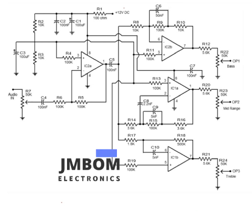
Circuit Diagram of 3-way Crossover Network
The design is straightforward and easy to integrate into modern amplifier systems.
Using LF353N in Audio Crossover Networks: Application Guide and Practical Tips
This circuit design makes use of two LF353N dual op-amp ICs. The incoming audio signal is first buffered by op-amp IC2a, with the gain level adjustable via potentiometer R7. After buffering, the audio signal is divided into three separate frequency bands using active filter stages built around IC2b, IC1a, and IC1b. Specifically, IC2b processes low frequencies (bass), IC1a handles midrange frequencies, and IC1b manages the high frequencies (treble). The tone of each band can be fine-tuned using R22 (bass), R23 (mid), and R24 (treble).
Key Setup Guidelines for 3-Way Crossover Network
Before building the crossover system, the following points should be considered for optimal performance:
- Use a high-quality PCB layout to minimize noise and improve overall audio fidelity.
- Power the circuit using a stable 12V DC supply.
- Install the LF353N ICs in IC sockets to allow for easy replacement or upgrades.
- Connect the outputs OP1, OP2, and OP3 to the appropriate inputs of a multi-channel power amplifier system.
Where to Use the LF353N Op-Amp: Applications
The LF353N op-amp is a versatile component with a wide range of practical uses, particularly where low noise and high performance are needed:
- Ideal for low-noise audio processing circuits
- Suitable for high input impedance amplifier designs
- Used in high-speed integrator circuits
- Commonly found in sample-and-hold circuits
- Supports fast digital-to-analog conversion (DAC) designs
- Also effective in any analog application that benefits from: Low input bias current Low offset voltage High input impedance Wide frequency response High slew rate
Summary
The LF353N, a dual JFET-input 8-pin op-amp, is widely used in audio applications due to its low input bias current, minimal offset voltage, and high input impedance. It also delivers excellent noise performance and minimal offset drift—making it a top choice for clean audio signal processing.
Question for you:
What other dual JFET op-amps are available on the market that could serve as alternatives to the LF353N?
LF351 Equivalent ICs and Common Op-Amp Questions Answered
What are the alternatives to the LF351 op-amp?
Several integrated circuits offer similar performance to the LF351. Common equivalents include the LM301, CA3140, TLC271, TLC071, ICL7611, TLC081, and NTE857M.
What is the LF353 op-amp used for?
The LF353 is suitable for a variety of analog signal processing applications. These include high-speed integrators, digital-to-analog converters (DACs), sample-and-hold circuits, and many other analog designs. It is rated for operation in the temperature range of 0°C to 70°C.
What does the LM358 op-amp do?
The LM358 is a dual operational amplifier IC that includes two independent op-amps powered by a single power source. It offers low power consumption and high gain-bandwidth, making it ideal for single-supply analog circuits. It’s commonly used in sensor interfaces, signal conditioning, and filtering applications.
What is the open-loop gain of the LF353?
According to the LF353 datasheet, the typical open-loop gain is around 100 V/mV, with a minimum of 25 V/mV. Under worst-case conditions (across temperature), the gain can drop to 15 V/mV.
Is there a difference between LM358 and LM358N?
Functionally, LM358 and LM358N are the same. The "N" suffix simply refers to the DIP (dual in-line package) version of the IC. There is no performance difference between the two.
Which op-amp is better: TL072 or NE5532?
It depends on the application. If your design involves higher frequency signals or requires greater bandwidth and faster slew rate, the NE5532 generally outperforms the TL072. However, TL072 may offer advantages in terms of input impedance and lower power consumption in some use cases.
What is the MCP23017 used for?
The MCP23017 is a 16-bit digital I/O expander that communicates via the I²C interface. It allows you to control up to 16 I/O pins using only two microcontroller pins, making it ideal for applications where GPIO expansion is needed without consuming extra MCU resources.
Is the LM358 suitable for audio applications?
The LM358 can be used in basic audio applications, especially where low power consumption is important. While it may not deliver audiophile-level performance compared to some higher-end op-amps, it is still a reliable choice for low-cost and low-power designs.
Are operational amplifiers still commonly used today?
Yes, op-amps remain a critical component in modern electronics. They are widely used in consumer products, industrial systems, and scientific instruments due to their versatility in analog circuit design.
Why is open-loop gain important in op-amps?
Open-loop gain plays a key role in determining the accuracy and stability of feedback-based op-amp circuits. While ideal op-amp analysis assumes infinite gain, real-world devices have finite gain, which affects the actual closed-loop gain and system performance.
Related Articles
TLV3201AQDCKRQ1 Comparator: Pinout, Operation, and Typical Uses
OPT3007 Ultra-Thin Ambient Light Sensor Overview and Applications
TPS7A26 LDO Regulator: Functionality and Key Applications
Guide to Low Dropout (LDO) Regulators and How They Work
ESP32-S3 Development Board: Pinout Diagram, Key Features, Technical Specs
DS18B20 Waterproof Temperature Sensor: Overview, Operation, and Common Uses

Amanda Miller
Amanda Miller is a senior electronics engineer with 6 years of experience. She focuses on studying resistors, transistors, and package design in detail. Her deep knowledge helps her bring innovation and high standards to the electronics industry.
Subscribe to JMBom Electronics !


