
onsemi 2N7002_NB9G002


- Part Number:
2N7002_NB9G002
- Manufacturer:
- Category:
- RoHs:
 Non-RoHS Compliant
 - Datasheet:
 2N7002_NB9G002_Datesheet
 - Description:
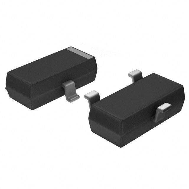
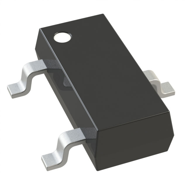
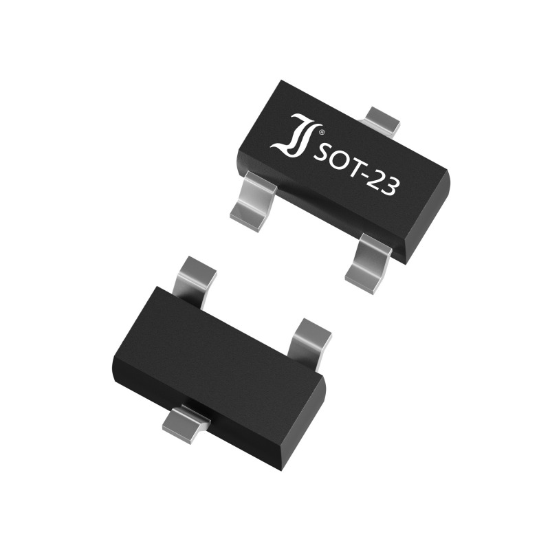
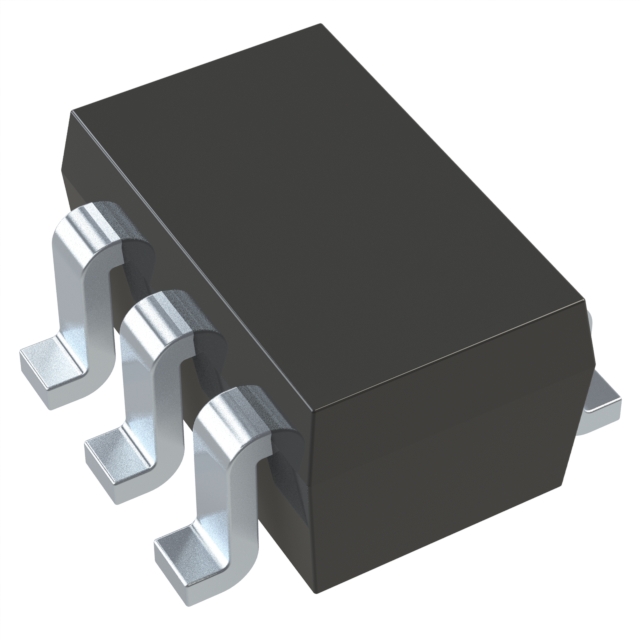
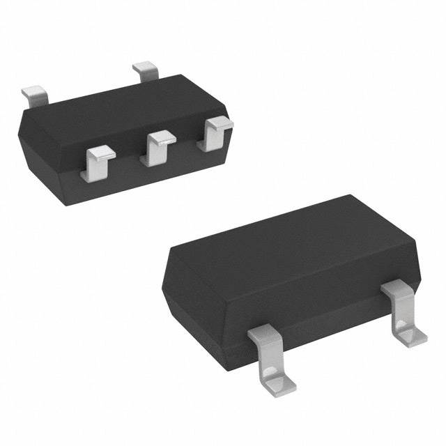
MOSFET N-CH 60V 115MA SOT-23
- In stock 0

2N7002_NB9G002 N-Channel Enhancement Mode Field Effect Transistor Data Sheet
Overview
- Part Number: 2N7002_NB9G002
- Type: N-Channel Enhancement Mode Field Effect Transistor (FET)
General Description and Features
- Produced using Fairchild's proprietary, high cell density, DMOS technology
- Designed to minimize on-state resistance while providing rugged, reliable, and fast switching performance
- Suitable for low voltage, low current applications such as small servo motor control, power MOSFET gate drivers, and other switching applications
- Features include high density cell design for low RDS(ON), voltage controlled small signal switch, rugged and reliable operation, and high saturation current capability
Absolute Maximum Ratings (TA = 25°C unless otherwise noted)
- Drain-Source Voltage (VDSS): 60 V
- Drain-Gate Voltage (VDGR): 60 V (RGS < 1 MΩ)
- Gate-Source Voltage (VGSS): ±20 V (Continuous), ±40 V (Non-Repetitive, tp < 50µs)
- Maximum Drain Current (ID): 115 mA (Continuous), 800 mA (Pulsed)
- Maximum Power Dissipation (PD): 200 mW
- Operating and Storage Temperature Range (TJ, TSTG): -65 to 150°C
- Maximum Lead Temperature for Soldering Purposes (TL): 300°C for 10 seconds at 1/16" from case
Thermal Characteristics
- Thermal Resistance, Junction-to-Ambient (RθJA): 625 °C/W
Electrical Characteristics (TA = 25°C unless otherwise noted)
OFF CHARACTERISTICS
- Drain-Source Breakdown Voltage (BVDSS): 60 V (VGS = 0 V, ID = 10 µA)
- Zero Gate Voltage Drain Current (IDSS): 1 µA (VDS = 48 V, VGS= 0 V) for 2N7000, 1 µA (TJ=125°C) for 2N7002, 1 µA (TJ=125°C) for NDS7002A
- Gate-Body Leakage, Forward (IGSSF): 10 nA (VGS = 15 V, VDS = 0 V) for 2N7000, 100 nA (VGS = 20 V, VDS = 0 V) for 2N7002, 100 nA (VGS = 20 V, VDS = 0 V) for NDS7002A
- Gate-Body Leakage, Reverse (IGSSR): -10 nA (VGS = -15 V, VDS = 0 V) for 2N7000, -100 nA (VGS = -20 V, VDS = 0 V) for 2N7002, -100 nA (VGS = -20 V, VDS = 0 V) for NDS7002A
ON CHARACTERISTICS
- Gate Threshold Voltage (VGS(th)): 1 V to 2.5 V (VDS = VGS, ID = 250 µA) for 2N7002, NDS7002A
- Static Drain-Source On-Resistance (RDS(ON)): 1.2 Ω to 7.5 Ω (VGS = 10 V, ID = 500 mA) for 2N7002, 1.2 Ω to 13.5 Ω (VGS = 10 V, ID = 500 mA) for NDS7002A
DYNAMIC CHARACTERISTICS
- Input Capacitance (Ciss): 20 pF to 50 pF (VDS = 25 V, VGS = 0 V, f = 1.0 MHz)
- Output Capacitance (Coss): 11 pF to 25 pF
- Reverse Transfer Capacitance (Crss): 4 pF to 5 pF
- Turn-On Time (ton): 10 ns to 20 ns (VDD = 15 V, RL = 25 Ω, ID = 500 mA, VGS = 10 V, RGEN = 25 Ω)
- Turn-Off Time (toff): 10 ns to 20 ns (VDD = 15 V, RL = 25 Ω, ID = 500 mA, VGS = 10 V, RGEN = 25 Ω)
Drain-Source Diode Characteristics and Maximum Ratings
- Maximum Continuous Drain-Source Diode Forward Current (IS): 115 mA for 2N7002, 280 mA for NDS7002A
- Maximum Pulsed Drain-Source Diode Forward Current (ISM): 0.8 A for 2N7002, 1.5 A for NDS7002A
- Drain-Source Diode Forward Voltage (VSD): 0.88 V to 1.5 V (VGS = 0 V, IS = 115 mA for 2N7002, IS = 400 mA for NDS7002A)
Purchase
No need to register to order from JMBom Electronics, but signing in lets you track your order like a pro. Give it a try for a smoother shopping ride.
Means
Easy peasy! Pay your way with PayPal, Credit Card, or wire transfer in USD. We've got you covered.
RFQ(Request for Quotations)
Get the freshest prices and stock updates by asking for a quote! Our sales team will shoot you an email within a day. It's that simple.
IMPORTANT NOTICE
1. Look out for your order details in your inbox! (If it's missing, check the spam folder just in case.)
2. Our sales manager will double-check the order and keep you posted on any price or stock changes. No worries, we've got you covered.

Shipping Rate
We ship orders once a day around 5 p.m., except Sunday. Once shipped, the estimated delivery time depends on the courier company you choose, usually 5-7 working days.

Shipping Methods
We provide DHL, FedEx, UPS, EMS, SF Express, and Registered Air Mail international shipping.


Payment
You can pay the orders on the website directly or pay by wire transfer offline. We support: Paypal、VISA、Credit Card.


onsemi
onsemi
onsemi
onsemi
onsemi
onsemi
onsemi
onsemi
onsemi
onsemi
onsemi

onsemi