
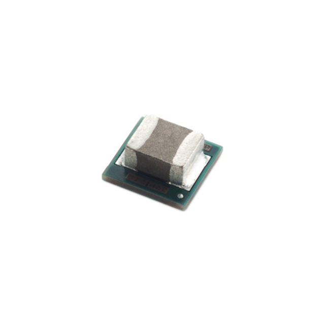
Texas Instruments LMZ14203TZX-ADJ/NOPB


- Part Number:
LMZ14203TZX-ADJ/NOPB
- Manufacturer:
- Category:
- RoHs:
 RoHS Compliant
 - Datasheet:
 LMZ14203TZX-ADJ/NOPB_Datesheet
 - Description:
Non-Isolated PoL Module DC DC Converter 1 Output 0.8 ~ 6V 3A 6V - 42V Input
- In stock 1,150

LMZ14203TZX-ADJ/NOPB – Complete Datasheet Summary
1. Basic Device Information
- Part Number: LMZ14203TZX-ADJ/NOPB
- Manufacturer: Texas Instruments
- Product Type: SIMPLE SWITCHER® 6–42V, 3A Step-Down Power Module
- Integrated: Shielded inductor, MOSFETs, controller, passives
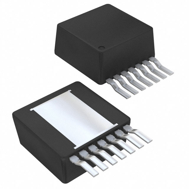
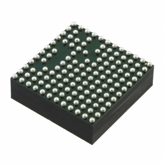
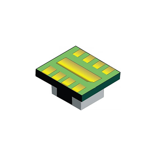
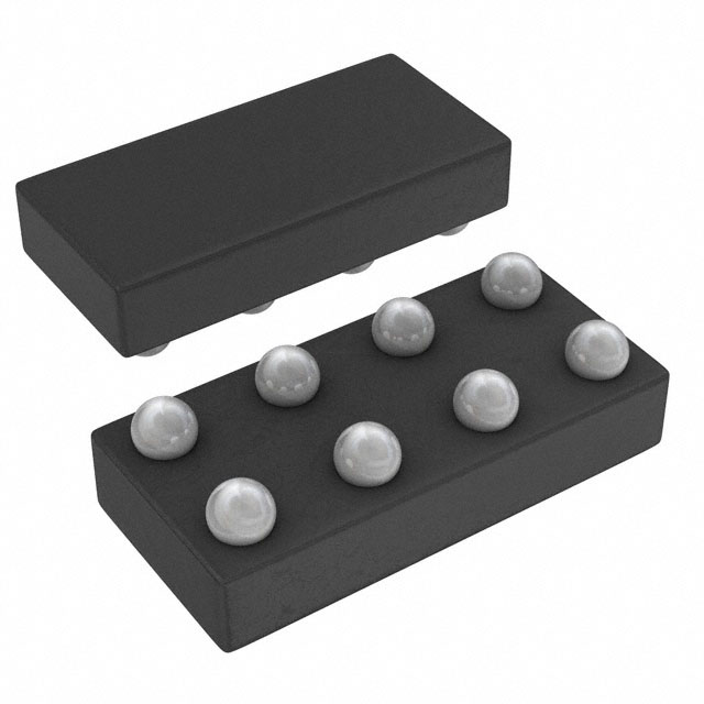
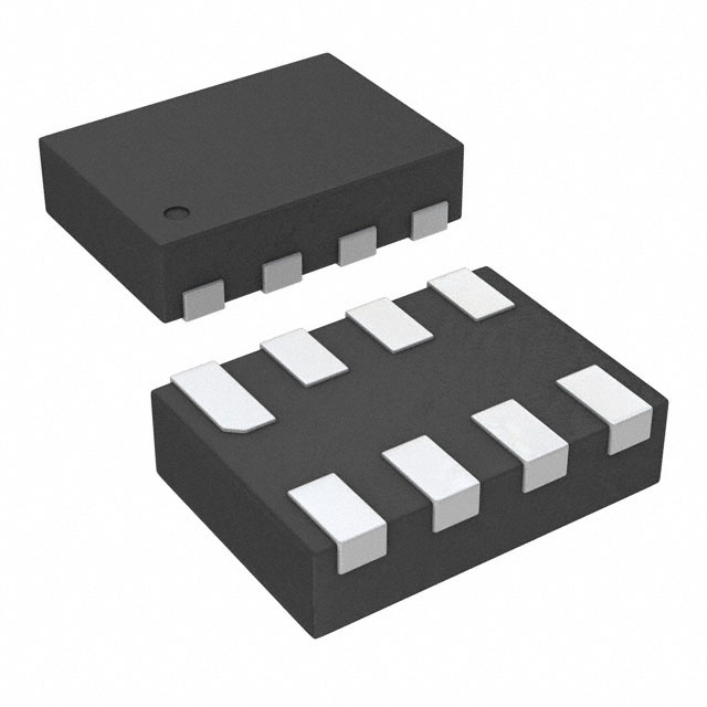
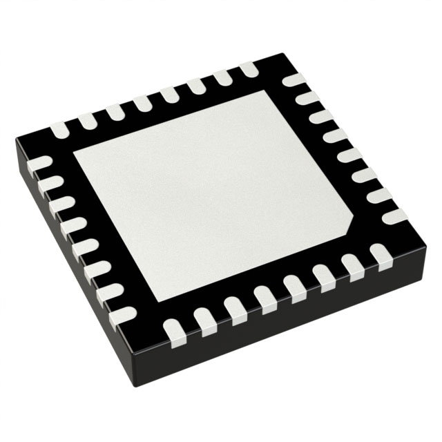
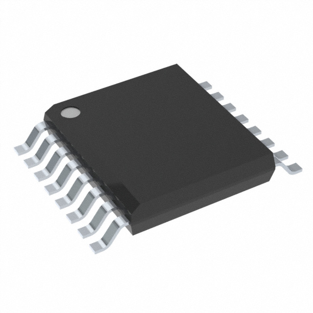
- Package: 7‑Pin TO‑PMOD (NDW package)
- Body Size: 10.16 mm × 9.85 mm
- Packaging: Large tape‑and‑reel, 500 units per reel
- RoHS: Compliant (NOPB = lead‑free)
- Moisture Sensitivity: MSL 3 (168 hr, 245°C peak reflow)
- Operating Junction Temp: −40°C to +125°C
- Control Scheme: Constant On‑Time (COT)
- Document: SNVS632S (Rev S, July 2017)
2. Key Features
- Wide input voltage: 6 V to 42 V
- Adjustable output: 0.8 V to 6 V
- Rated output current: 3 A
- Up to 90% efficiency
- Integrated shielded inductor for low EMI
- Meets EN55022 Class B radiated emissions
- Precision enable with programmable UVLO
- Adjustable soft‑start
- Internal protection: OVP, OCP, UVLO, thermal shutdown
- Prebiased start‑up capability
- Minimal external components: 3 resistors + 4 capacitors
- Pin‑to‑pin compatible with LMZ14201/202 family
3. Electrical Specifications
表格
| Parameter | Min | Typ | Max | Unit |
|---|---|---|---|---|
| Input Voltage (VIN) | 6 | — | 42 | V |
| Output Voltage (VOUT) | 0.8 | — | 6 | V |
| Output Current | — | — | 3 | A |
| Feedback Reference (VFB) | 0.784 | 0.804 | 0.825 | V |
| Enable Threshold (rising) | 1.1 | 1.18 | 1.25 | V |
| Enable Hysteresis | — | 90 | — | mV |
| Current Limit (typical) | 3.2 | 4.2 | 5.25 | A |
| Thermal Shutdown | — | 165 | — | °C |
| Shutdown Quiescent Current | — | — | 25 | µA |
| Output Ripple | — | 8 | — | mVpp |
| Line Regulation | — | 0.01 | — | % |
| Load Regulation | — | 1.5 | — | mV/A |
4. Absolute Maximum Ratings
- VIN, RON to GND: −0.3 V to +43.5 V
- EN, FB, SS to GND: −0.3 V to +7 V
- Junction Temperature: 150°C
- Storage Temperature: −65°C to +150°C
- Peak Reflow Temperature: 245°C
- ESD (HBM): ±2000 V
5. Thermal Data
- RθJA (4‑layer PCB): 19.3°C/W
- RθJA (2‑layer PCB): 21.5°C/W
- RθJC (top): 1.9°C/W
- Exposed pad must be soldered to GND for thermal performance
6. Pin Configuration (7‑Pin TO‑PMOD, Top View)
表格
| Pin No. | Name | Function |
|---|---|---|
| 1 | VIN | Power input (6–42 V) |
| 2 | RON | Sets on‑time / switching frequency |
| 3 | EN | Precision enable input |
| 4 | GND | System ground |
| 5 | SS | Soft‑start control |
| 6 | FB | Feedback sense input |
| 7 | VOUT | Power output |
| EP | Exposed Pad | GND (internally tied to Pin 4) |
7. Functional Description
- COT Control: Fast transient response; no external compensation
- Current Mode: Cycle‑by‑cycle current limit
- DCM/CCM Operation: Light load DCM for high efficiency; heavy load CCM
- OVP: FB > 0.92 V clamps output
- Thermal Shutdown: Activates at 165°C; releases at ~145°C
- Soft‑Start: 8 µA current source charges CSS to control ramp rate
- Zero Current Detect: Prevents reverse inductor current in DCM
8. External Component Design
Output Voltage Set
VOUT = 0.8 V × (1 + RFBT / RFBB)
- RFBT = top feedback resistor
- RFBB = bottom feedback resistor
- Feedforward capacitor CFF parallel with RFBT improves transient response
Switching Frequency
RON resistor programs fSW up to 1 MHz
tON(min) = 150 ns; tOFF(min) = 260 ns
Soft‑Start
tSS = (0.8 V × CSS) / 8 µA
- Recommended CSS ≥ 22 nF (tSS ≥ 2.2 ms)
Input/Output Capacitors
- CIN: ≥10 µF X7R, low ESR, close to VIN
- COUT: ≥10 µF X7R; 100 µF recommended for 3A loads
9. Recommended Operating Conditions
- VIN: 6 V to 42 V
- IOUT: 0 A to 3 A
- TA: −40°C to +105°C (ambient)
- TJ: −40°C to +125°C (junction)
10. Typical Applications
- 12V / 24V / 36V Industrial Point‑of‑Load
- Automotive and factory automation
- Test and measurement equipment
- Space‑constrained high‑thermal systems
- Negative output voltage designs (AN‑2027)
- FPGA/ASIC/MCU power supplies
11. Layout Guidelines
- Exposed pad soldered to GND plane with thermal vias
- CIN placed extremely close to VIN–GND
- Minimize high di/dt loop area
- Feedback resistors close to FB pin; away from SW noise
- Wide VIN/VOUT traces; dedicated ground for analog signals
12. Ordering & Packaging
- LMZ14203TZX‑ADJ/NOPB: 7‑pin TO‑PMOD, 500/tape‑and‑reel, −40 to 125°C
- Marking: LMZ14203 TZ‑ADJ
- Reel: 500 units, diameter 330 mm, width 24.4 mm
- Pin‑1 quadrant: Q2
Purchase
No need to register to order from JMBom Electronics, but signing in lets you track your order like a pro. Give it a try for a smoother shopping ride.
Means
Easy peasy! Pay your way with PayPal, Credit Card, or wire transfer in USD. We've got you covered.
RFQ(Request for Quotations)
Get the freshest prices and stock updates by asking for a quote! Our sales team will shoot you an email within a day. It's that simple.
IMPORTANT NOTICE
1. Look out for your order details in your inbox! (If it's missing, check the spam folder just in case.)
2. Our sales manager will double-check the order and keep you posted on any price or stock changes. No worries, we've got you covered.

Shipping Rate
We ship orders once a day around 5 p.m., except Sunday. Once shipped, the estimated delivery time depends on the courier company you choose, usually 5-7 working days.

Shipping Methods
We provide DHL, FedEx, UPS, EMS, SF Express, and Registered Air Mail international shipping.


Payment
You can pay the orders on the website directly or pay by wire transfer offline. We support: Paypal、VISA、Credit Card.


Texas Instruments
Texas Instruments
Texas Instruments
Texas Instruments
Texas Instruments
Texas Instruments
Texas Instruments
Texas Instruments
Texas Instruments
Texas Instruments
Texas Instruments

Texas Instruments