
Texas Instruments TPS22916BYFPR


- Part Number:
TPS22916BYFPR
- Manufacturer:
- Category:
- RoHs:
 RoHS Compliant
 - Datasheet:
 TPS22916BYFPR_Datesheet
 - Description:
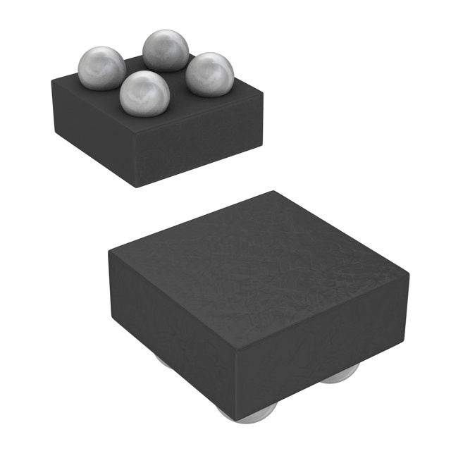
Power Switch/Driver 1:1 P-Channel 2A 4-DSBGA
- In stock 59,546

TPS22916BYFPR Product Information
Product Overview
The TPS22916BYFPR is a 1-V to 5.5-V, 2-A, 60-mΩ ultra-low leakage load switch designed for applications requiring minimal power loss and efficient power management. Manufactured by Texas Instruments, this device features a low ON-resistance P-Channel MOSFET and advanced gate control design, making it suitable for a wide range of portable and wearable devices.
Features
- Input Operating Voltage Range (VIN): 1 V to 5.5 V
- Maximum Continuous Current (IMAX): 2 A
- ON-Resistance (RON):60 mΩ (typ.) at 5 V100 mΩ (typ.) at 1.8 V200 mΩ (typ.) at 1 V
- Ultra-low Power Consumption:ON state (IQ): 0.5 μA (typ.), 1 μA (max.)OFF state (ISD): 10 nA (typ.), 100 nA (max.)
- Smart ON Pin Pulldown (RPD):ON ≥ VIH (ION): 10 nA (max.)ON ≤ VIL (RPD): 750 kΩ (typ.)
- Slow Timing in C Version Limits Inrush Current:5-V turn-on time (tON): 1400 μs at 5 mV/μs1.8-V turn-on time (tON): 3000 μs at 1 mV/μs1-V turn-on time (tON): 6500 μs at 0.3 mV/μs
- Fast Timing in B Version Reduces Wait Time:5-V turn-on time (tON): 115 μs at 57 mV/μs1.8-V turn-on time (tON): 250 μs at 12 mV/μs1-V turn-on time (tON): 510 μs at 3.3 mV/μs
- Always-ON True Reverse Current Blocking (RCB):Activation current (IRCB): –500 mA (typ.)Reverse leakage (IIN, RCB): –300 nA (max.)
- Quick Output Discharge (QOD): 150 Ω (typ.) (N version has no QOD)
- Active Low Enable Option (L versions)
Applications
- Wearables
- Smartphones
- Tablets
- Portable speakers
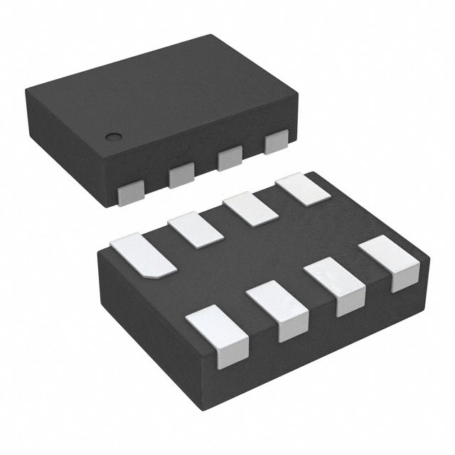
Pin Configuration
Pin Functions
TableCopy
| Pin Number | Pin Name | Type | Function |
|---|---|---|---|
| A1 | VOUT | Power | Switch output |
| A2 | VIN | Power | Switch input |
| B1 | GND | Ground | Device ground |
| B2 | ON | Digital input | Device enable |
Ordering Information
- Part Number: TPS22916BYFPR
- Package Type: DSBGA (YFP)
- Package Drawing: YFP
- Pins: 4
- SPQ (Standard Pack Quantity): 3000
- Reel Diameter: 180.0 mm
- Reel Width: 8.4 mm
- A0: 0.86 mm
- B0: 0.86 mm
- K0: 0.59 mm
- P1: 4.0 mm
- W: 8.0 mm
- Pin1 Quadrant: Q1
Absolute Maximum Ratings
- Input Voltage (VIN): –0.3 V to 6 V
- Output Voltage (VOUT): –0.3 V to 6 V
- Enable Voltage (VON): –0.3 V to 6 V
- Maximum Continuous Switch Current (IMAX): 2 A
- Maximum Pulsed Switch Current (IPLS): 2.5 A (pulse < 300-µs, 2% duty cycle)
- Maximum Junction Temperature (TJ,MAX): 125 °C
- Storage Temperature (TSTG): –65 °C to 150 °C
- Maximum Lead Temperature (TLEAD): 300 °C (10-s soldering time)
ESD Ratings
- Human-body model (HBM), per ANSI/ESDA/JEDEC JS-001: ±2000 V
- Charged-device model (CDM), per JEDEC specification JESD22-C101: ±500 V
Recommended Operating Conditions
- Input Voltage (VIN): 1 V to 5.5 V
- Output Voltage (VOUT): 0 V to 5.5 V
- High-level Input Voltage (VIH): 1 V to 5.5 V
- Low-level Input Voltage (VIL): 0 V to 0.35 V
- Operating Free-Air Temperature (TA): –40 °C to 85 °C
Thermal Information
- Junction-to-Ambient Thermal Resistance (θJA): 193 °C/W
- Junction-to-Case (Top) Thermal Resistance (θJCtop): 2.3 °C/W
- Junction-to-Board Thermal Resistance (θJB): 36 °C/W
- Junction-to-Top Characterization Parameter (ψJT): 12 °C/W
- Junction-to-Board Characterization Parameter (ψJB): 36 °C/W
Electrical Characteristics
Input Supply (VIN)
- Quiescent Current (I Q, VIN IN): 0.5 μA (typ.), 1 μA (max.) at 25 °C
- Shutdown Current (I SD, VIN IN): 10 nA (typ.), 100 nA (max.) at 25 °C
ON-Resistance (RON)
- VIN = 5 V: 60 mΩ (typ.), 80 mΩ (max.) at 25 °C
- VIN = 3.6 V: 70 mΩ (typ.), 90 mΩ (max.) at 25 °C
- VIN = 1.8 V: 100 mΩ (typ.), 125 mΩ (max.) at 25 °C
- VIN = 1.2 V: 150 mΩ (typ.), 200 mΩ (max.) at 25 °C
- VIN = 1 V: 200 mΩ (typ.), 275 mΩ (max.) at 25 °C
Enable Pin (ON)
- ON Pin Leakage Current (I ON): 10 nA (max.) at 25 °C
- Smart Pulldown Resistance (RPD): 750 kΩ (typ.) at 25 °C
Reverse Current Blocking (RCB)
- RCB Activation Current (IRCB): –500 mA (typ.) at 25 °C
- RCB Activation Time (t RCB): 10 μs (typ.) at 25 °C
- RCB Release Voltage (V RCB): 25 mV (typ.) at 25 °C
- Reverse Leakage Current (I IN, RCB): –300 nA (max.) at 25 °C
Quick Output Discharge (QOD)
- QOD Output Discharge Resistance: 150 Ω (typ.) at 25 °C
Switching Characteristics
Fast Timing (TPS22916B)
- Turn-On Time (tON):5 V: 115 μs at 57 mV/μs3.6 V: 140 μs at 12 mV/μs1.8 V: 250 μs at 12 mV/μs1.2 V: 350 μs at 3.3 mV/μs1 V: 510 μs at 3.3 mV/μs
- Rise Time (tRISE):5 V: 70 μs3.6 V: 80 μs1.8 V: 130 μs1.2 V: 190 μs
Purchase
No need to register to order from JMBom Electronics, but signing in lets you track your order like a pro. Give it a try for a smoother shopping ride.
Means
Easy peasy! Pay your way with PayPal, Credit Card, or wire transfer in USD. We've got you covered.
RFQ(Request for Quotations)
Get the freshest prices and stock updates by asking for a quote! Our sales team will shoot you an email within a day. It's that simple.
IMPORTANT NOTICE
1. Look out for your order details in your inbox! (If it's missing, check the spam folder just in case.)
2. Our sales manager will double-check the order and keep you posted on any price or stock changes. No worries, we've got you covered.

Shipping Rate
We ship orders once a day around 5 p.m., except Sunday. Once shipped, the estimated delivery time depends on the courier company you choose, usually 5-7 working days.

Shipping Methods
We provide DHL, FedEx, UPS, EMS, SF Express, and Registered Air Mail international shipping.


Payment
You can pay the orders on the website directly or pay by wire transfer offline. We support: Paypal、VISA、Credit Card.


Texas Instruments
Texas Instruments
Texas Instruments
Texas Instruments
Texas Instruments
Texas Instruments
Texas Instruments
Texas Instruments
Texas Instruments
Texas Instruments
Texas Instruments

Texas Instruments