
onsemi NTS4001NT1G


- Part Number:
NTS4001NT1G
- Manufacturer:
- Category:
- RoHs:
 RoHS Compliant
 - Datasheet:
 NTS4001NT1G_Datesheet
 - Description:
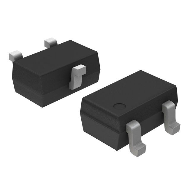
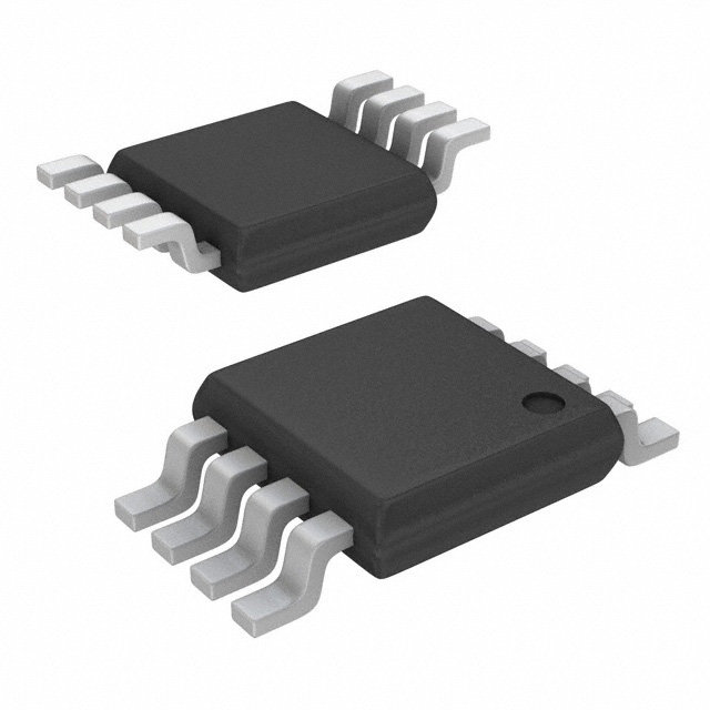
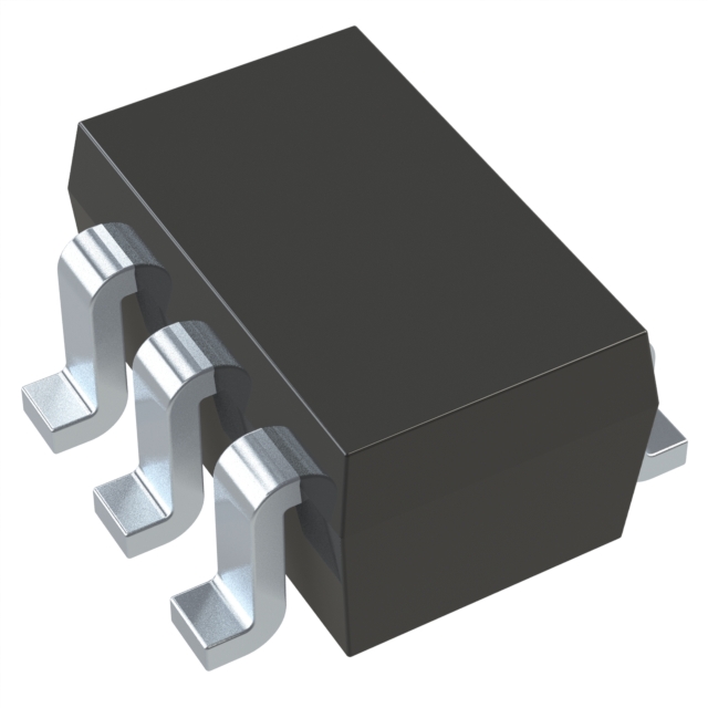
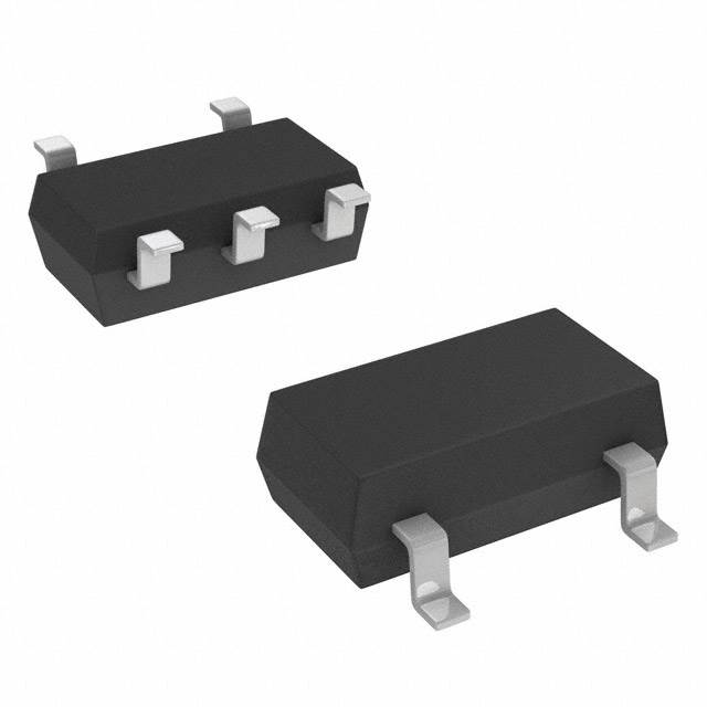
MOSFET N-CH 30V 270MA SC70-3
- In stock 42,720

NTS4001NT1G: Technical Specifications and Details
Overview
The NTS4001NT1G is a single N-Channel MOSFET designed for small signal applications. This product is manufactured by onsemi (formerly ON Semiconductor) and is RoHS compliant and Pb-Free. The data sheet was last revised in June 2019.
Features
- Low Gate Charge for Fast Switching
- Small Footprint (30% Smaller than TSOP-6)
- ESD Protected Gate
- AEC-Q101 Qualified and PPAP Capable (NVS4001N)
- Pb-Free and RoHS Compliant
Applications
- Low Side Load Switch
- Li-Ion Battery Supplied Devices (Cell Phones, PDAs, DSC)
- Buck Converters
- Level Shifts
Maximum Ratings (TJ = 25°C unless otherwise stated)
| Parameter | Symbol | Value | Units |
|---|---|---|---|
| Drain-to-Source Voltage | VDSS | 30 | V |
| Gate-to-Source Voltage | VGS | ±20 | V |
| Continuous Drain Current (TA = 25°C) | ID | 270 | mA |
| Continuous Drain Current (TA = 85°C) | ID | 200 | mA |
| Power Dissipation (TA = 25°C) | PD | 330 | mW |
| Pulsed Drain Current (t = 10 µs) | IDM | 800 | mA |
| Operating Junction and Storage Temperature | TJ, TSTG | -55 to 150 | °C |
| Source Current (Body Diode) | IS | 270 | mA |
| Lead Temperature for Soldering Purposes (1/8” from case for 10 s) | TL | 260 | °C |
Electrical Characteristics (TJ = 25°C unless otherwise stated)
| Parameter | Symbol | Test Condition | Min | Typ | Max | Unit |
|---|---|---|---|---|---|---|
| Drain-to-Source Breakdown Voltage | V(BR)DSS | VGS = 0 V, ID = 100 µA | 30 | - | - | V |
| Drain-to-Source Breakdown Voltage Temperature Coefficient | V(BR)DSS/TJ | - | 60 | - | - | mV/°C |
| Zero Gate Voltage Drain Current | IDSS | VGS = 0 V, VDS = 30 V | - | - | 1.0 | µA |
| Gate-to-Source Leakage Current | IGSS | VDS = 0 V, VGS = ±10 V | - | - | ±1.0 | µA |
| Gate Threshold Voltage | VGS(TH) | VGS = VDS, ID = 100 µA | 0.8 | 1.2 | 1.5 | V |
| Gate Threshold Temperature Coefficient | VGS(TH)/TJ | - | -3.4 | - | - | mV/°C |
| Drain-to-Source On Resistance (VGS = 4.0 V, ID = 10 mA) | RDS(on) | - | 1.0 | 1.5 | - | Ω |
| Drain-to-Source On Resistance (VGS = 2.5 V, ID = 10 mA) | RDS(on) | - | 1.5 | 2.0 | - | Ω |
| Forward Transconductance | gFS | VDS = 3.0 V, ID = 10 mA | - | 80 | - | mS |
| Input Capacitance | CISS | VGS = 0 V, f = 1.0 MHz, VDS = 5.0 V | 20 | 33 | - | pF |
| Output Capacitance | COSS | - | 19 | 32 | - | pF |
| Reverse Transfer Capacitance | CRSS | - | 7.25 | 12 | - | pF |
| Total Gate Charge | QG(TOT) | VGS = 5.0 V, VDS = 24 V, ID = 0.1 A | 0.9 | 1.3 | - | nC |
| Threshold Gate Charge | QG(TH) | - | 0.2 | - | - | nC |
| Gate-to-Source Charge | QGS | - | 0.3 | - | - | nC |
| Gate-to-Drain Charge | QGD | - | 0.2 | - | - | nC |
Switching Characteristics (Note 3)
| Parameter | Symbol | Test Condition | Min | Typ | Max | Unit |
|---|---|---|---|---|---|---|
| Turn-On Delay Time | td(ON) | VGS = 4.5 V, VDD = 5.0 V, ID = 10 mA, RG = 50 Ω | - | 17 | - | ns |
| Rise Time | tr | - | - | 23 | - | ns |
| Turn-Off Delay Time | td(OFF) | - | - | 94 | - | ns |
| Fall Time | tf | - | - | 82 | - | ns |
Drain-Source Diode Characteristics
| Parameter | Symbol | Test Condition | Min | Typ | Max | Unit |
|---|---|---|---|---|---|---|
| Forward Diode Voltage (TJ = 25°C) | VSD | VGS = 0 V, IS = 10 mA | 0.65 | 0.7 | - | V |
| Forward Diode Voltage (TJ = 125°C) | VSD | VGS = 0 V, IS = 10 mA | 0.43 | - | - | V |
| Reverse Recovery Time | tRR | VGS = 0 V, dIS/dt = 8.0 A/µs, IS = 10 mA | - | 5.0 | - | ns |
Mechanical Dimensions
| Dimension | Value (mm) | Value (Inches) |
|---|---|---|
| Length (L) | 2.00 ± 0.10 | 0.079 ± 0.004 |
| Width (W) | 1.20 ± 0.10 | 0.047 ± 0.004 |
| Thickness (T) | 0.90 ± 0.10 | 0.035 ± 0.004 |
| A1 | 0.00 to 0.10 | 0.000 to 0.004 |
| A2 | 0.70 REF | 0.028 REF |
| b | 0.30 to 0.40 | 0.012 to 0.016 |
| c | 0.10 to 0.25 | 0.004 to 0.010 |
| D | 1.80 to 2.20 | 0.071 to 0.087 |
| E | 1.15 to 1.35 | 0.045 to 0.053 |
| e | 1.20 to 1.40 | 0.047 to 0.055 |
| e1 | 0.65 BSC | 0.026 BSC |
| HE | 0.035 to 0.040 | 0.001 to 0.002 |
Ordering Information
- Part Number: NTS4001NT1G
- Package: SC-70 (Pb-Free)
- Quantity: 3000 / Tape & Reel
Marking Diagram
- Device Code: TD
- Date Code: M
- Pb-Free Indicator: G or microdot (�)
Important Notice
- Commercial-Off-The-Shelf (COTS) Products: Suitable for Commercial, Industrial, and Automotive Applications.
- Not for High-Reliability Applications: Not specifically designed for Military, Aviation, Aerospace, Life-Dependent Medical applications, or any application requiring high reliability.
- Contact onsemi: For applications requiring high reliability and/or presenting an extreme operating environment, written consent and authorization from onsemi is required.
Purchase
No need to register to order from JMBom Electronics, but signing in lets you track your order like a pro. Give it a try for a smoother shopping ride.
Means
Easy peasy! Pay your way with PayPal, Credit Card, or wire transfer in USD. We've got you covered.
RFQ(Request for Quotations)
Get the freshest prices and stock updates by asking for a quote! Our sales team will shoot you an email within a day. It's that simple.
IMPORTANT NOTICE
1. Look out for your order details in your inbox! (If it's missing, check the spam folder just in case.)
2. Our sales manager will double-check the order and keep you posted on any price or stock changes. No worries, we've got you covered.

Shipping Rate
We ship orders once a day around 5 p.m., except Sunday. Once shipped, the estimated delivery time depends on the courier company you choose, usually 5-7 working days.

Shipping Methods
We provide DHL, FedEx, UPS, EMS, SF Express, and Registered Air Mail international shipping.


Payment
You can pay the orders on the website directly or pay by wire transfer offline. We support: Paypal、VISA、Credit Card.


onsemi
onsemi
onsemi
onsemi
onsemi
onsemi
onsemi
onsemi
onsemi
onsemi
onsemi

onsemi