
NXP USA Inc. P82B96TD,112


- Part Number:
P82B96TD,112
- Manufacturer:
- Category:
- RoHs:
 RoHS Compliant
 - Datasheet:
 P82B96TD,112_Datesheet
 - Description:
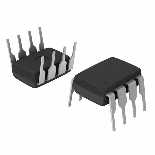
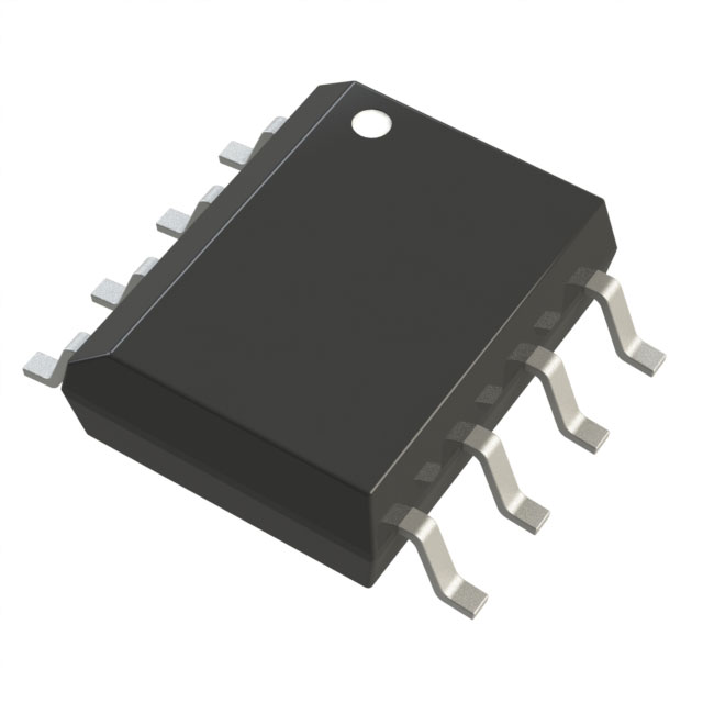
Buffer, ReDriver 2 Channel 400kHz 8-SO
- In stock 44,696

P82B96TD,112 Datasheet Summary
Product Overview
- Family: Dual Bidirectional Bus Buffer
- Model: P82B96
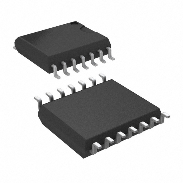
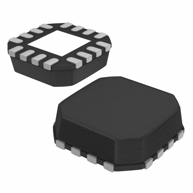
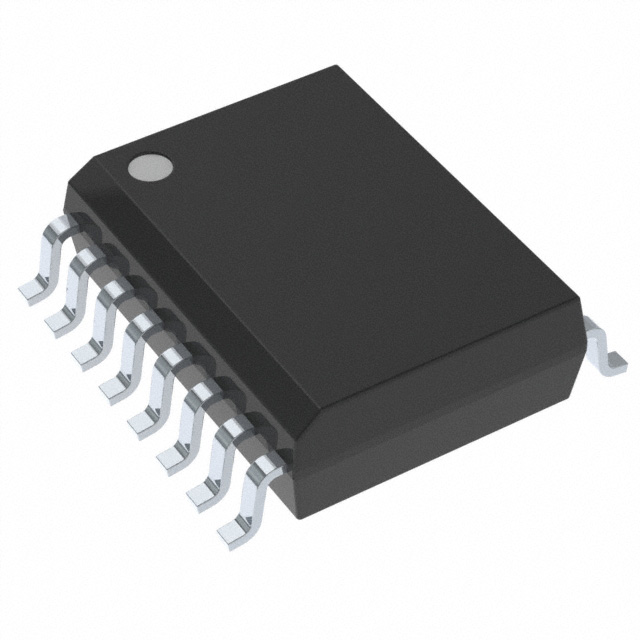
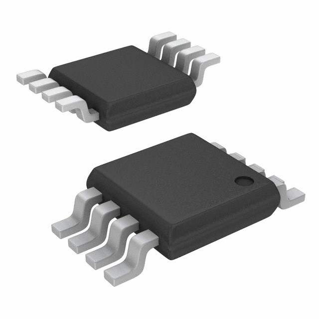
- Package: SO8
- Orderable Part Number: P82B96TD,118
Key Features
- Bidirectional Data Transfer: Supports I2C-bus signals.
- Isolation of Capacitance: Allows 400 pF on Sx/Sy side and 4000 pF on Tx/Ty side.
- Sink Capability: Tx/Ty outputs have 60 mA sink capability for driving low-impedance or high capacitive buses.
- High-Speed Operation: Supports 400 kHz operation over at least 20 meters of wire.
- Wide Supply Voltage Range: 2 V to 15 V with I2C-bus logic levels on Sx/Sy side independent of supply voltage.
- Low Power Supply Current: Ensures energy efficiency.
- ESD Protection: Exceeds 3500 V HBM per JESD22-A114 and 1000 V CDM per JESD22-C101.
- Latch-up Free: Bipolar process with no latching structures.
- Packages Offered: SO8 and TSSOP8.
Applications
- Interface Between I2C-Buses: Operating at different logic levels (e.g., 5 V and 3 V or 15 V).
- Interface Between I2C-Bus and SMBus: Standard 350 µA SMBus.
- Conversion of I2C-Bus Signals: To multi-drop differential bus hardware.
- Opto-Isolation: Between I2C-bus nodes up to 400 kHz.
Ordering Information
- Package Type: SO8
- Topside Marking: P82B96T
- Orderable Part Number: P82B96TD,118
- Packing Method: REEL 13" Q1/T1 NDP
- Minimum Order Quantity: 2500
- Temperature Range: Tamb = -40 °C to +85 °C
Pin Configuration
- Sx: I2C-bus (SDA or SCL)
- Rx: Receive signal
- Tx: Transmit signal
- GND: Negative supply
- Ty: Transmit signal
- Ry: Receive signal
- Sy: I2C-bus (SDA or SCL)
- VCC: Positive supply voltage
Limiting Values
- Supply Voltage (VCC): -0.3 V to +18 V
- Voltage on Pin Sx (VSx): -0.3 V to +18 V
- Voltage on Pin Tx (VTx): -0.3 V to +18 V
- Voltage on Pin Rx (VRx): -0.3 V to +18 V
- In Current on Any Pin: 250 mA
- Total Power Dissipation (Ptot): 300 mW
- Junction Temperature Operating Range: -40 °C to +125 °C (P82B96TD/S900)
- Storage Temperature (Tstg): -55 °C to +125 °C
- Ambient Temperature Operating (Tamb): -40 °C to +85 °C
Characteristics
- Supply Voltage Operating (VCC): 2.0 V to 15 V
- Bus HIGH Voltage (VSx, VSy): 0.9 V to 1.8 V
- Supply Current (ICC): 1.1 mA to 2.5 mA
- Additional Quiescent Supply Current per Tx or Ty LOW: 1.7 mA to 3.5 mA
- Maximum Input/Output Voltage (VSx, VSy): 15 V
- Static Output Loading on I2C-bus (ISx, ISy): 0.2 mA to 3 mA
- Dynamic Output Sink Capability on I2C-bus (ISx, ISy): 7 mA to 18 mA
- Leakage Current on I2C-bus (ISx, ISy): 1 µA to 10 µA
- Maximum Output Voltage Level (VTx, VTy): 15 V
- Static Output Loading on Buffered Bus (ITx, ITy): 30 mA
- Dynamic Output Sink Capability, Buffered Bus (ITx, ITy): 60 mA to 100 mA
- Leakage Current on Buffered Bus (ITx, ITy): 1 µA to 10 µA
- Input Current from I2C-bus (ISx, ISy): -1 µA to -10 µA
- Input Current from Buffered Bus (IRx, IRy): -1 µA to -10 µA
- Leakage Current on Buffered Bus Input (IRx, IRy): 1 µA to 10 µA
- Output Logic LOW Level (VSx, VSy): 0.8 V to 0.88 V (at 0.2 mA), 670 mV to 790 mV (at 3 mA)
- Input Logic Switching Threshold Voltages (VSx, VSy): 600 mV to 700 mV
- Input Logic HIGH Level Fraction of Applied VCC (VRx, VRy): 0.58VCC
- Input Threshold Fraction of Applied VCC (VRx, VRy): 0.5VCC
- Input Logic LOW Level Fraction of Applied VCC (VRx, VRy): 0.42VCC
- Logic Level Threshold Difference (VSx, VSy): 50 mV to 85 mV
- Thermal Resistance (Rth(j-pcb)): 127 K/W
Functional Description
The P82B96 provides a non-latching, bidirectional, logic interface between the normal I2C-bus and a range of other bus configurations. It interfaces I2C-bus logic signals to similar buses having different voltage and current levels without any restrictions on the normal I2C-bus protocols or clock speed. The IC adds minimal loading to the I2C-bus node, and loadings of the new bus or remote I2C-bus nodes are not transmitted or transformed to the local node.
Application Information
- Interfacing Different Logic Levels: The P82B96 can interface an I2C-bus type of bus with different logic levels.
- Galvanic Isolation: Interfaces with opto-couplers to provide opto-isolation between I2C-bus nodes up to 400 kHz.
- Long Distance Communications: Supports long distance I2C-bus communications using buffered bus signals.
- Extending a DDC Bus: Can extend a DDC bus using buffered bus signals and appropriate circuitry.
Purchase
No need to register to order from JMBom Electronics, but signing in lets you track your order like a pro. Give it a try for a smoother shopping ride.
Means
Easy peasy! Pay your way with PayPal, Credit Card, or wire transfer in USD. We've got you covered.
RFQ(Request for Quotations)
Get the freshest prices and stock updates by asking for a quote! Our sales team will shoot you an email within a day. It's that simple.
IMPORTANT NOTICE
1. Look out for your order details in your inbox! (If it's missing, check the spam folder just in case.)
2. Our sales manager will double-check the order and keep you posted on any price or stock changes. No worries, we've got you covered.

Shipping Rate
We ship orders once a day around 5 p.m., except Sunday. Once shipped, the estimated delivery time depends on the courier company you choose, usually 5-7 working days.

Shipping Methods
We provide DHL, FedEx, UPS, EMS, SF Express, and Registered Air Mail international shipping.


Payment
You can pay the orders on the website directly or pay by wire transfer offline. We support: Paypal、VISA、Credit Card.


NXP USA Inc.
NXP USA Inc.
NXP USA Inc.
NXP USA Inc.
NXP USA Inc.
NXP USA Inc.
NXP USA Inc.
NXP USA Inc.
NXP USA Inc.
NXP USA Inc.
NXP USA Inc.
NXP USA Inc.