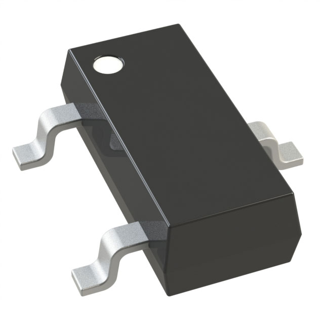
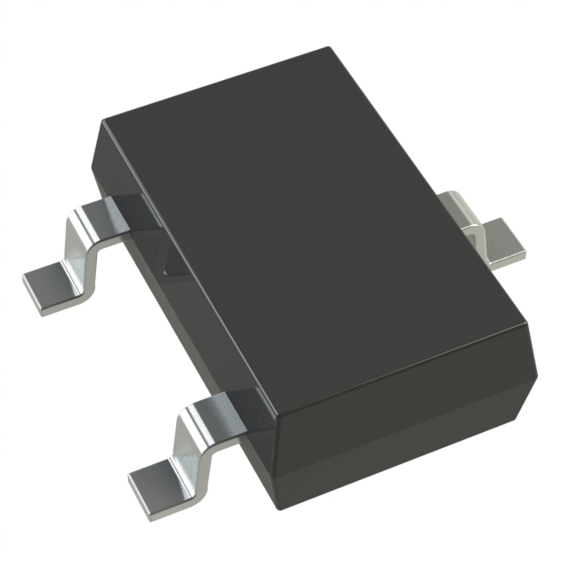
Infineon Technologies PTFB193408SVV1XWSA1


- Part Number:
PTFB193408SVV1XWSA1
- Manufacturer:
- Category:
- RoHs:
 Non-RoHS Compliant
 - Datasheet:
 PTFB193408SVV1XWSA1_Datesheet
 - Description:
RF MOSFET LDMOS 30V H-34275G-6
- In stock 0
Infineon PTFB193408SVV1XWSA1 Product Information
Product Overview
The PTFB193408SVV1XWSA1 is a high-power RF LDMOS FET designed for multi-standard cellular power amplifier applications in the 1930 to 1990 MHz frequency band. This device offers excellent thermal performance, high gain, and integrated input/output matching, making it suitable for demanding applications.
Key Features
- High Power Output: 340W
- Frequency Range: 1930–1990 MHz
- Supply Voltage: 30V
- Broadband Internal Matching: For efficient operation across the frequency band
- Wide Video Bandwidth: Ensures high performance in various applications
- Single-Carrier WCDMA Performance:Output Power: 100WEfficiency: 33%Gain: 19.0 dBPAR: 7.5 dB @ 0.01% CCDFACPR @ 5MHz: –35 dBc
- Increased Negative Gate-Source Voltage Range: For improved performance in Doherty amplifiers
- Handling Capability: 10:1 VSWR at 30V, 340W (CW) output power
- Integrated ESD Protection: Ensures robustness against electrostatic discharge
- Excellent Thermal Stability: Ensures reliable operation under varying conditions
- RoHS-Compliant: Environmentally friendly design
Ordering Information
- Part Number: PTFB193408SVV1XWSA1
- Package: H-34275G-6/2, ceramic open-cavity, formed leads, earless
- Shipping: Tape & Reel, 250 pcs
RF Characteristics
Single-Carrier WCDMA Measurements (tested in Infineon test fixture)
- Conditions: VDD = 30V, IDQ = 2.65A, POUT = 80W average, f = 1990MHz
- Signal: 3GPP, 3.84MHz channel bandwidth, with 10dB peak/average @ 0.01% CCDF
- TableCopy
| Characteristic | Symbol | Min | Typ | Max | Unit |
|---|---|---|---|---|---|
| Gain | Gps | 18 | 19 | — | dB |
| Drain Efficiency | nD | 29 | 31 | — | % |
| Adjacent Channel Power Ratio | ACPR | — | -32 | -30 | dBc |
Two-Carrier WCDMA Characteristics (not subject to production test—verified by design/characterization in Infineon test fixture)
- Conditions: VDD = 30V, IDQ = 2.6A, POUT = 80W average, f1 = 1980MHz, f2 = 1990MHz
- Signal: 3GPP, 3.84MHz channel bandwidth, 8.0dB peak/average @ 0.01% CCDF
- TableCopy
| Characteristic | Symbol | Min | Typ | Max | Unit |
|---|---|---|---|---|---|
| Gain | Gps | — | 19.5 | — | dB |
| Drain Efficiency | nD | — | 29 | — | % |
| Intermodulation Distortion | IMD | — | -33 | — | dBc |
Two-Tone Characteristics (not subject to production test—verified by design/characterization in Infineon test fixture)
- Conditions: VDD = 30V, IDQ = 2.6A, POUT = 265W PEP, f = 1990MHz, tone spacing = 1MHz
- TableCopy
| Characteristic | Symbol | Min | Typ | Max | Unit |
|---|---|---|---|---|---|
| Gain | Gps | — | 19.5 | — | dB |
| Drain Efficiency | nD | — | 36 | — | % |
| Intermodulation Distortion | IMD | — | -30 | — | dBc |
DC Characteristics
Conditions: VGS = 0V, VDS = 30V, IDQ = 2.6A
TableCopy
| Characteristic | Symbol | Min | Typ | Max | Unit |
|---|---|---|---|---|---|
| Drain-Source Breakdown Voltage | V(BR)DSS | 65 | — | — | V |
| Drain Leakage Current | IDSS | — | — | 1.0 | µA |
| On-State Resistance | RDS(on) | — | 0.05 | — | Ω |
| Operating Gate Voltage | VGS | 2.3 | 2.8 | 3.3 | V |
| Gate Leakage Current | IGSS | — | — | 1.0 | µA |
Maximum Ratings
TableCopy
| Parameter | Symbol | Value | Unit |
|---|---|---|---|
| Drain-Source Voltage | VDsS | 65 | V |
| Gate-Source Voltage | VGS | -6 to +10 | V |
| Junction Temperature | TJ | 200 | ℃ |
| Storage Temperature Range | TSTG | -40 to +150 | ℃ |
| Thermal Resistance (TcAsE=70C, 300 W CW) | RoJC | 0.2 | C/W |
Package Outline Specifications
- Package Type: H-34275G-6/2 (formed leads)
- Dimensions:Length: 30.61 mm [1.205 inches]Width: 22.22 mm [0.875 inches]Height: 10.16 mm [0.400 inches]
- Lead Thickness: 0.13 mm ± 0.051 mm [0.005 inches ± 0.002 inches]
- Gold Plating Thickness: 0.25 micron [10 microinches]
Pinout Diagram
- V1, V2: VDD
- G1, G2: Gate
- D1, D2: Drain
- S: Source (flange)
Reference Circuit
- Input Components:Capacitors: 1 µF, 10 µF, 18 pF, 1.5 pF, 1,000 pFInductors: 22 nHResistors: 10 Ω, 100 Ω, 1,300 Ω, 1,200 Ω
- Output Components:Capacitors: 220 µF, 4.7 µF, 10 µF
Revision History
- Rev. 03 (2015-10-01): Updated data sheet with new performance characteristics and package information.
Legal Disclaimer
The information in this document is provided as a guide and should not be considered a guarantee of conditions or characteristics. Infineon Technologies disclaims any and all warranties and liabilities of any kind, including warranties of non-infringement of intellectual property rights of any third party.
Purchase
No need to register to order from JMBom Electronics, but signing in lets you track your order like a pro. Give it a try for a smoother shopping ride.
Means
Easy peasy! Pay your way with PayPal, Credit Card, or wire transfer in USD. We've got you covered.
RFQ(Request for Quotations)
Get the freshest prices and stock updates by asking for a quote! Our sales team will shoot you an email within a day. It's that simple.
IMPORTANT NOTICE
1. Look out for your order details in your inbox! (If it's missing, check the spam folder just in case.)
2. Our sales manager will double-check the order and keep you posted on any price or stock changes. No worries, we've got you covered.

Shipping Rate
We ship orders once a day around 5 p.m., except Sunday. Once shipped, the estimated delivery time depends on the courier company you choose, usually 5-7 working days.

Shipping Methods
We provide DHL, FedEx, UPS, EMS, SF Express, and Registered Air Mail international shipping.


Payment
You can pay the orders on the website directly or pay by wire transfer offline. We support: Paypal、VISA、Credit Card.


Infineon Technologies
Infineon Technologies
Infineon Technologies
Infineon Technologies

Infineon Technologies
Infineon Technologies

Infineon Technologies

Infineon Technologies

Infineon Technologies
Infineon Technologies
Infineon Technologies
Infineon Technologies

