
Nexperia USA Inc. 74ALVCH16601DGGY


- Part Number:
74ALVCH16601DGGY
- Manufacturer:
- Category:
- RoHs:
 RoHS Compliant
 - Datasheet:
 74ALVCH16601DGGY_Datesheet
 - Description:
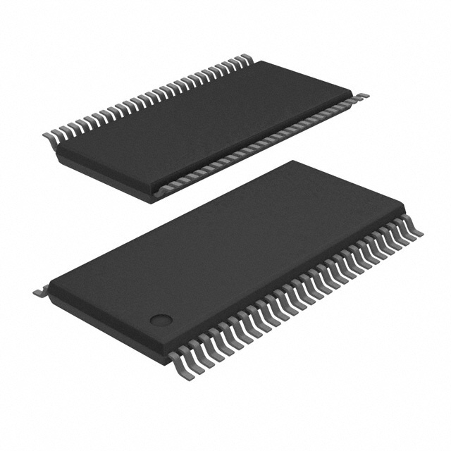
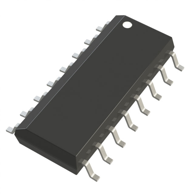
IC UNIV BUS TXRX 18BIT 56TSSOP
- In stock 0

74ALVCH16601DGGY Device Information
Ordering Information
TableCopy
| Parameter | Description | Value |
|---|---|---|
| Type Number | Device identifier | 74ALVCH16601DGGY |
| Package | Physical package type | TSSOP56 (SOT364-1) |
| Temperature Range | Operating temperature range | -40°C to +85°C |
| Package Description | Detailed package description | Plastic thin shrink small outline package; 56 leads; body width 6.1 mm |
Pinning Information
TableCopy
| Symbol | Pin Number | Description |
|---|---|---|
| A0-A17 | 3, 5, 6, 8, 9, 10, 12, 13, 14, 15, 16, 17, 19, 20, 21, 23, 24, 26 | Data inputs/outputs |
| B0-B17 | 54, 52, 51, 49, 48, 47, 45, 44, 43, 42, 41, 40, 38, 37, 36, 34, 33, 31 | Data outputs/inputs |
| OEAB | 1 | A-to-B output enable input (active LOW) |
| OEBA | 27 | B-to-A output enable input (active LOW) |
| LEAB | 2 | A-to-B latch enable input (active HIGH) |
| LEBA | 28 | B-to-A latch enable input (active HIGH) |
| CPAB | 55 | A-to-B clock input (active HIGH) |
| CPBA | 30 | B-to-A clock input (active HIGH) |
| CEAB | 56 | A-to-B clock enable input (active LOW) |
| CEBA | 29 | B-to-A clock enable input (active LOW) |
| GND | 4, 11, 18, 25, 32, 39, 46, 53 | Ground (0 V) |
| Vcc | 7, 22, 35, 50 | Supply voltage |
Functional Description
The 74ALVCH16601DGGY is an 18-bit universal bus transceiver with 3-state outputs. Data flow in each direction is controlled by output enable (OEAB and OEBA), latch enable (LEAB and LEBA), clock enable (CEAB and CEBA), and clock (CPAB and CPBA) inputs. The device supports transparent mode, latch mode, and clocked data transfer modes.
Limiting Values
TableCopy
| Parameter | Min | Max | Unit |
|---|---|---|---|
| Supply Voltage (Vcc) | -0.5 | +4.6 | V |
| Input Voltage (data inputs) | -0.5 | Vcc + 0.5 | V |
| Input Voltage (control inputs) | -0.5 | +4.6 | V |
| Output Voltage (vo) | -0.5 | Vcc + 0.5 | V |
| Input Clamping Current (IK) | -50 | - | mA |
| Output Clamping Current (lok) | - | ±50 | mA |
| Supply Current (Icc) | - | 100 | mA |
| Ground Current (GND) | -100 | - | mA |
| Storage Temperature (Tstg) | -65 | +150 | °C |
| Total Power Dissipation (Ptot) | - | 500 | mW |
Recommended Operating Conditions
TableCopy
| Parameter | Min | Max | Unit |
|---|---|---|---|
| Supply Voltage (Vcc) | 2.3 | 3.6 | V |
| Input Voltage (v) | 0 | Vcc | V |
| Output Voltage (vo) | 0 | Vcc | V |
| Ambient Temperature (Tamb) | -40 | +85 | °C |
| Input Transition Rise and Fall Rate (△t/△V) | 0 | 20 | ns/V (Vcc = 2.3V to 3.0V) |
| Input Transition Rise and Fall Rate (△t/△V) | 0 | 10 | ns/V (Vcc = 3.0V to 3.6V) |
Static Characteristics
TableCopy
| Parameter | Conditions | Min | Typ | Max | Unit |
|---|---|---|---|---|---|
| HIGH-level Input Voltage (VIH) | Vcc = 2.3 to 2.7 V | 1.7 | 1.2 | - | V |
| HIGH-level Input Voltage (VIH) | Vcc = 2.7 to 3.6 V | 2.0 | 1.5 | - | V |
| LOW-level Input Voltage (VIL) | Vcc = 2.3 to 2.7 V | - | 1.2 | 0.7 | V |
| LOW-level Input Voltage (VIL) | Vcc = 2.7 to 3.6 V | - | 1.5 | 0.8 | V |
| HIGH-level Output Voltage (VOH) | IO = -100 μA; Vcc = 2.3 V to 3.6 V | Vcc - 0.2 | Vcc | - | V |
| LOW-level Output Voltage (VOL) | IO = 100 μA; Vcc = 2.3 V to 3.6 V | - | GND | 0.20 | V |
| Input Leakage Current (II) | VI = Vcc or GND; Vcc = 2.3 V to 3.6 V | - | 0.1 | 5 | μA |
| Supply Current (ICC) | Vcc = 2.3 to 3.6 V; VI = Vcc or GND; IO = 0 A | - | 150 | 750 | μA |
Dynamic Characteristics
TableCopy
| Parameter | Conditions | Min | Typ | Max | Unit |
|---|---|---|---|---|---|
| Propagation Delay (tpd) | Vcc = 2.3 V to 2.7 V | 1.0 | 3.1 | 5.2 | ns |
| Propagation Delay (tpd) | Vcc = 2.7 V | - | 3.1 | 4.7 | ns |
| Propagation Delay (tpd) | Vcc = 3.0 V to 3.6 V | 1.0 | 2.8 | 4.2 | ns |
| Enable Time (ten) | Vcc = 2.3 V to 2.7 V | 1.1 | 3.1 | 5.3 | ns |
| Disable Time (tdis) | Vcc = 2.3 V to 2.7 V | 1.4 | 2.8 | 4.9 | ns |
| Set-up Time (tsu) | Vcc = 2.3 V to 2.7 V | 2.3 | -0.2 | - | ns |
| Hold Time (th) | Vcc = 2.3 V to 2.7 V | 1.2 | 0.3 | - | ns |
Package Outline
- Package Type: TSSOP56 (SOT364-1)
- Body Width: 6.1 mm
- Lead Count: 56 leads
Abbreviations
TableCopy
| Acronym | Description |
|---|---|
| CDM | Charged Device Model |
| CMOS | Complementary Metal-Oxide Semiconductor |
| DUT | Device Under Test |
| ESD | ElectroStatic Discharge |
| HBM | Human Body Model |
| TTL | Transistor-Transistor Logic |
Purchase
No need to register to order from JMBom Electronics, but signing in lets you track your order like a pro. Give it a try for a smoother shopping ride.
Means
Easy peasy! Pay your way with PayPal, Credit Card, or wire transfer in USD. We've got you covered.
RFQ(Request for Quotations)
Get the freshest prices and stock updates by asking for a quote! Our sales team will shoot you an email within a day. It's that simple.
IMPORTANT NOTICE
1. Look out for your order details in your inbox! (If it's missing, check the spam folder just in case.)
2. Our sales manager will double-check the order and keep you posted on any price or stock changes. No worries, we've got you covered.

Shipping Rate
We ship orders once a day around 5 p.m., except Sunday. Once shipped, the estimated delivery time depends on the courier company you choose, usually 5-7 working days.

Shipping Methods
We provide DHL, FedEx, UPS, EMS, SF Express, and Registered Air Mail international shipping.


Payment
You can pay the orders on the website directly or pay by wire transfer offline. We support: Paypal、VISA、Credit Card.


Nexperia USA Inc.
Nexperia USA Inc.
Nexperia USA Inc.
Nexperia USA Inc.
Nexperia USA Inc.
Nexperia USA Inc.
Nexperia USA Inc.
Nexperia USA Inc.
Nexperia USA Inc.
Nexperia USA Inc.
Nexperia USA Inc.
Nexperia USA Inc.