
onsemi BSS84LT1


- Part Number:
BSS84LT1
- Manufacturer:
- Category:
- RoHs:
 Non-RoHS Compliant
 - Datasheet:
 BSS84LT1_Datesheet
 - Description:
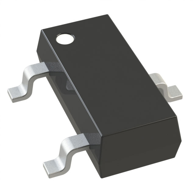
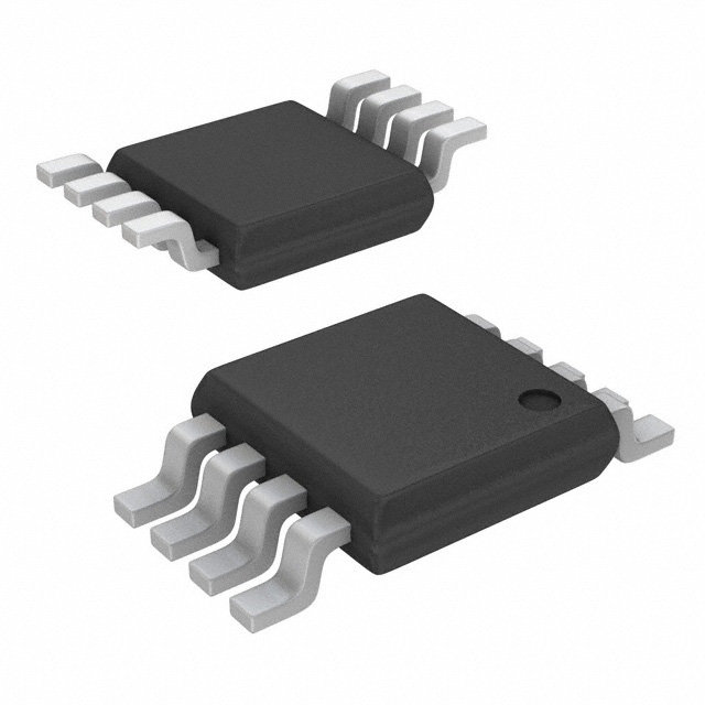
MOSFET P-CH 50V 130MA SOT-23
- In stock 0

BSS84LT1 Product Summary
Basic Information
- Part Number: BSS84LT1
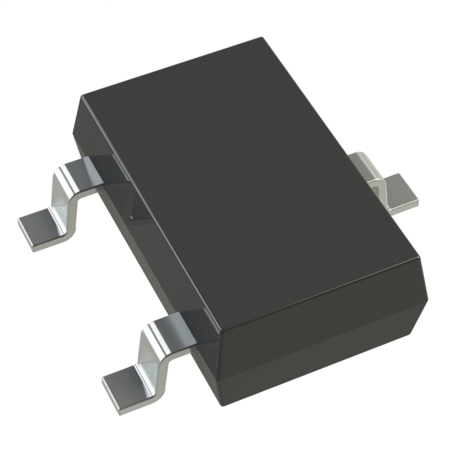
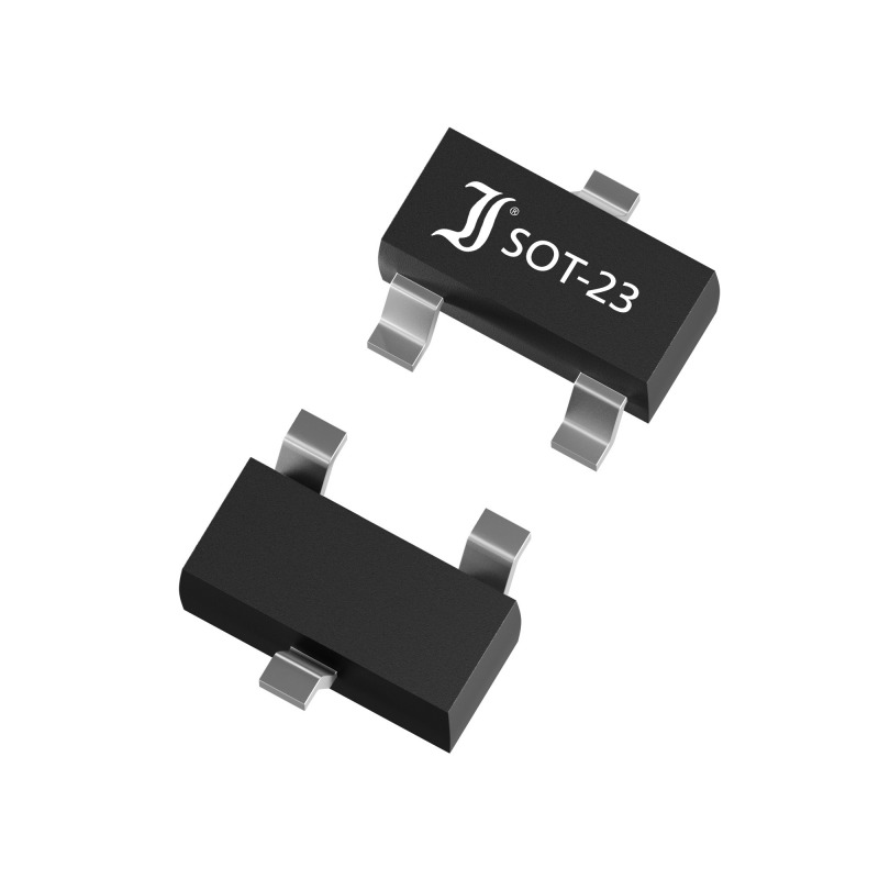
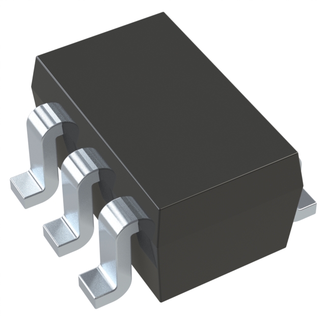
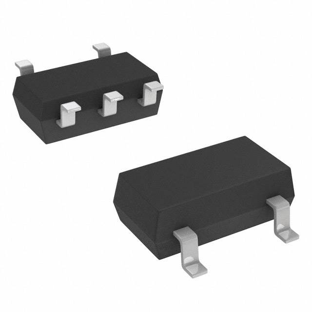
- Package Type: SOT-23 (Pb-Free)
- Shipping Quantity: 3000 per Tape & Reel
- Case Style: CASE 318 STYLE 21
General Description
The BSS84LT1 is a single P-Channel MOSFET designed for power applications. It features a SOT-23 surface mount package, which saves board space. The device is suitable for automotive and other applications requiring unique site and control change requirements, and is AEC-Q101 qualified and PPAP capable. The BSS84LT1 is Pb-Free and RoHS compliant.
Features
- Drain-Source Voltage (VDSS): -50 Vdc
- Drain Current (ID):Continuous: -130 mAPulsed: -520 mA
- On-State Resistance (RDS(on)): 10 Ω @ VGS = -10 V
- Miniature SOT-23 Surface Mount Package
- Automotive Grade: BV Prefix for Automotive and Other Applications Requiring Unique Site and Control Change Requirements; AEC-Q101 Qualified and PPAP Capable
- RoHS Compliance: Pb-Free
Marking Diagram & Pin Assignment
- Device Code: PD
- Date Code: M
- Pb-Free Package Indicator: �
- Pin Configuration:Pin 1: GatePin 2: SourcePin 3: Drain
Ordering Information
- BSS84LT1G: SOT-23 (Pb-Free), 3000 per Tape & Reel
- BVSS84LT1G: SOT-23 (Pb-Free), 3000 per Tape & Reel
- SBSS84LT1G: SOT-23 (Pb-Free), 3000 per Tape & Reel
- BSS84LT7G: SOT-23 (Pb-Free), 3500 per Tape & Reel
Maximum Ratings (@TJ = 25°C, unless otherwise noted)
- Drain-Source Voltage (VDSS): -50 Vdc
- Gate-Source Voltage (VGS): ±20 Vdc
- Drain Current (ID):Continuous: -130 mAPulsed: -520 mA
- Total Power Dissipation (PD): 225 mW
- Operating and Storage Temperature Range (TJ, TSTG): -55 to +150 °C
- Thermal Resistance, Junction-to-Ambient (RθJA): 556 °C/W
- Maximum Lead Temperature for Soldering Purposes (TL): 260 °C
Electrical Characteristics (@TA = 25°C, unless otherwise noted)
- OFF CHARACTERISTICS:Drain-Source Breakdown Voltage (V(BR)DSS): -50 V (VGS = 0 V, ID = -250 µA)Zero Gate Voltage Drain Current (IDSS):VDS = -25 V, VGS = 0 V: -0.1 µAVDS = -50 V, VGS = 0 V: -15 µAVDS = -50 V, VGS = 0 V, TJ = 125°C: -60 µAGate-Body Leakage Current (IGSS): ±10 nA (VGS = ±20 V, VDS = 0 V)
- ON CHARACTERISTICS:Gate-Source Threshold Voltage (VGS(th)): -0.9 to -2.0 V (VDS = VGS, ID = -250 µA)Static Drain-Source On-Resistance (RDS(on)): 4.7 to 10 Ω (VGS = -5.0 V, ID = -100 mA)Transfer Admittance (|yfs|): 50 mS (VDS = -25 V, ID = -100 mA, f = 1.0 kHz)
- DYNAMIC CHARACTERISTICS:Input Capacitance (Ciss): 36 pF (VDS = 5.0 V)Output Capacitance (Coss): 17 pFTransfer Capacitance (Crss): 6.5 pF
- SWITCHING CHARACTERISTICS:Turn-On Delay Time (td(on)): 3.6 ns (VDD = -15 V, ID = -2.5 A, RL = 50 Ω)Rise Time (tr): 9.7 nsTurn-Off Delay Time (td(off)): 12 nsFall Time (tf): 1.7 nsGate Charge (QT): 2.2 nC (VDD = -40 V, ID = -0.5 A, VGS = -10 V)
- SOURCE-DRAIN DIODE CHARACTERISTICS:Continuous Current (IS): -0.130 APulsed Current (ISM): -0.520 AForward Voltage (VSD): -2.2 V (VGS = 0 V, IS = -130 mA)
Typical Electrical Characteristics
- Transfer Characteristics: See Figure 1
- On-Region Characteristics: See Figure 2
- On-Resistance versus Drain Current: See Figures 3, 4
- On-Resistance Variation with Temperature: See Figure 5
- Gate Charge: See Figure 6
- Body Diode Forward Voltage: See Figure 7
Mechanical Case Outline Package Dimensions
- SOT-23 (TO-236): 2.90x1.30x1.00 mm
- Pin Configuration:Pin 1: GatePin 2: SourcePin 3: Drain
Purchase
No need to register to order from JMBom Electronics, but signing in lets you track your order like a pro. Give it a try for a smoother shopping ride.
Means
Easy peasy! Pay your way with PayPal, Credit Card, or wire transfer in USD. We've got you covered.
RFQ(Request for Quotations)
Get the freshest prices and stock updates by asking for a quote! Our sales team will shoot you an email within a day. It's that simple.
IMPORTANT NOTICE
1. Look out for your order details in your inbox! (If it's missing, check the spam folder just in case.)
2. Our sales manager will double-check the order and keep you posted on any price or stock changes. No worries, we've got you covered.

Shipping Rate
We ship orders once a day around 5 p.m., except Sunday. Once shipped, the estimated delivery time depends on the courier company you choose, usually 5-7 working days.

Shipping Methods
We provide DHL, FedEx, UPS, EMS, SF Express, and Registered Air Mail international shipping.


Payment
You can pay the orders on the website directly or pay by wire transfer offline. We support: Paypal、VISA、Credit Card.


onsemi
onsemi
onsemi
onsemi
onsemi
onsemi
onsemi
onsemi
onsemi
onsemi
onsemi

onsemi