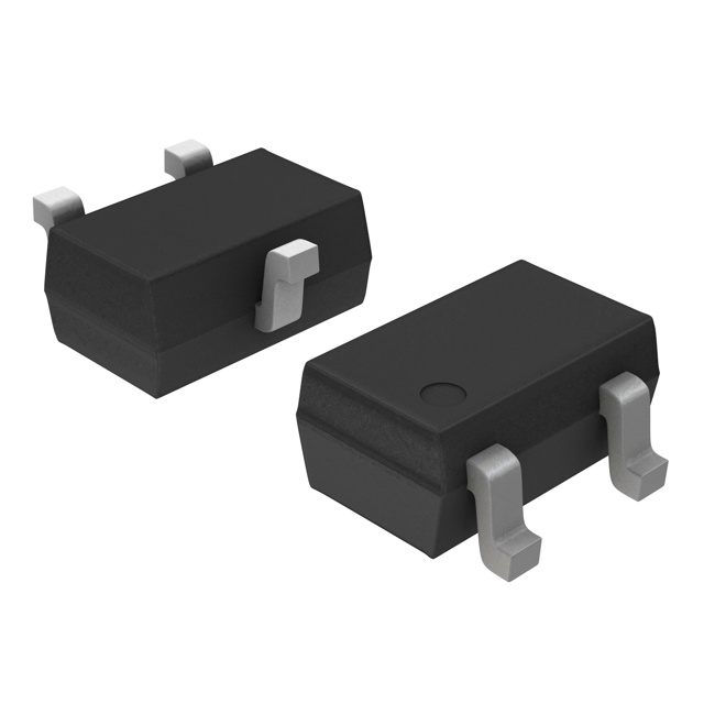
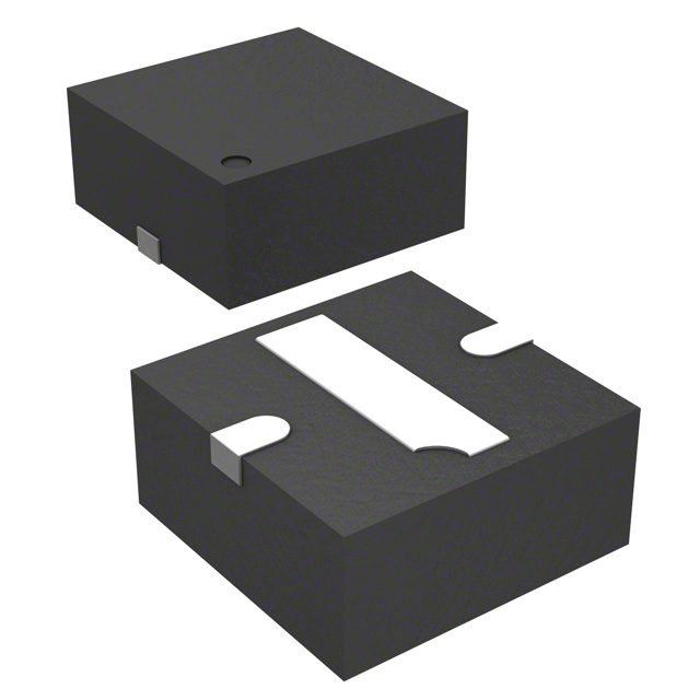
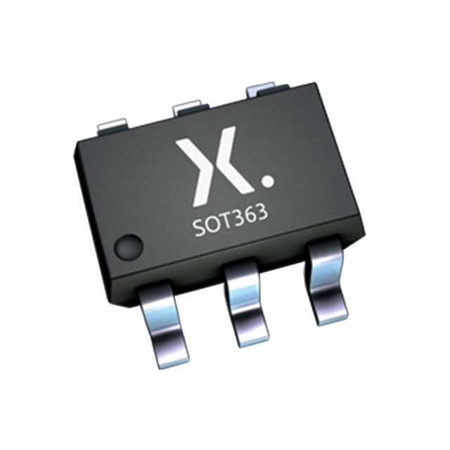
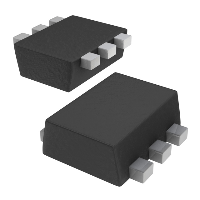
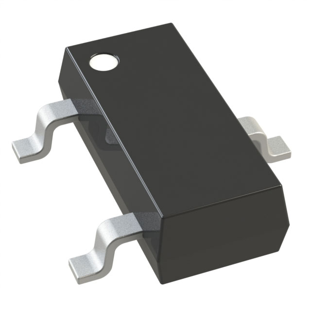
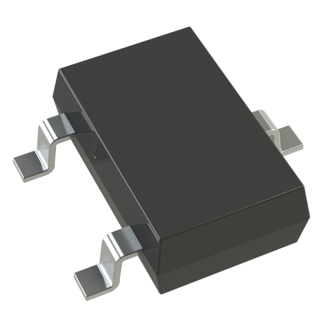
onsemi MUN5113T1


- Part Number:
MUN5113T1
- Manufacturer:
- Category:
- RoHs:
 Non-RoHS Compliant
 - Datasheet:
 MUN5113T1_Datesheet
 - Description:
TRANS PREBIAS PNP 50V SC70-3
- In stock 0
MUN5113T1 – Complete Datasheet Summary
50 V, 100 mA PNP Digital Bias-Resistor Transistor, 47 kΩ + 47 kΩ, SC-70, 3 k-pc Reel
1. Device Identity
- Type: PNP silicon “digital transistor” with monolithic bias-resistor network
- Base part: MUN5113T1 (tape-and-reel suffix “T1” = 7-inch / 3 000-unit reel)
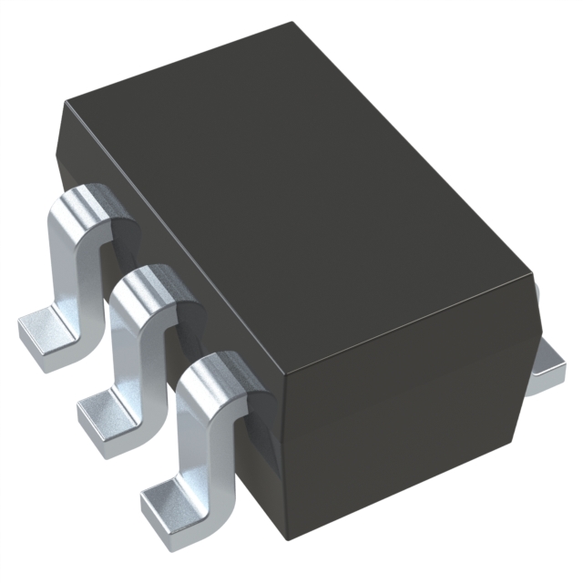
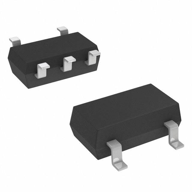
- Package: SC-70 (SOT-323) 3-lead, Pb-free, halogen-free, RoHS compliant
- Automotive option: add prefix “S” (SMUN5113T1) or “NSV” (NSVMUN5113T1) – AEC-Q101 qualified & PPAP capable
2. Internal Circuit & Pin-out
        R1 = 47 kΩ
  Pin 1 (BASE/INPUT) ───■─── BASE PNP
        R2 = 47 kΩ
               ├─── Pin 2 (EMITTER/GND)
  Pin 3 (COLLECTOR/OUTPUT)
- Pin 1: Base / digital input
- Pin 2: Emitter / ground
- Pin 3: Collector / switched output
3. Absolute Maximum Ratings (TA = 25 °C)
| Parameter | Symbol | Rating | Unit |
|---|---|---|---|
| Collector-base voltage | VCBO | 50 | V |
| Collector-emitter voltage | VCEO | 50 | V |
| Collector current | IC | 100 | mA |
| Device dissipation (Note 1) | PD | 202 | mW |
| Junction temperature | TJ | 150 | °C |
| Storage temperature | Tstg | –55 … +150 | °C Note 1: FR-4 minimum pad; derate 1.6 mW/°C above 25 °C. |
4. Thermal Characteristics
| Parameter | Symbol | Typ | Max | Unit |
|---|---|---|---|---|
| Junction-to-ambient (min pad) | RθJA | — | 618 | °C/W |
| Junction-to-ambient (1-inch pad) | RθJA | — | 403 | °C/W |
| Junction-to-lead | RθJL | — | 280 | °C/W |
5. Electrical Characteristics (TA = 25 °C unless noted)
OFF CHARACTERISTICS
| Parameter | Test Condition | Min | Typ | Max | Unit |
|---|---|---|---|---|---|
| Collector cut-off | VCB = 50 V, IE = 0 | — | — | 100 | nA |
| Collector-emitter cut-off | VCE = 50 V, IB = 0 | — | — | 500 | nA |
| Emitter-base cut-off | VEB = 6 V, IC = 0 | — | — | 0.1 | µA |
ON CHARACTERISTICS (pulse test 300 µs, 2 % duty)
| Parameter | Condition | Min | Typ | Max | Unit |
|---|---|---|---|---|---|
| DC current gain hFE | VCE = 10 V, IC = 5 mA | 80 | — | 250 | — |
| Collector-emitter saturation | IC = 10 mA, IB = 1 mA | — | — | 0.25 | V |
| Output low voltage (digital) | VCC = 5 V, VB = 0.5 V, RL = 1 kΩ | — | — | 0.2 | V |
| Output high leakage | VCC = 5 V, VB = 5.5 V, RL = 1 kΩ | 4.9 | — | — | V |
RESISTOR NETWORK
| Resistor | Nominal | Tolerance |
|---|---|---|
| R1 (base-series) | 47 kΩ | ±20 % |
| R2 (base-emitter) | 47 kΩ | ±20 % |
| Ratio R1/R2 | 1.0 | 0.8 … 1.2 |
6. Typical Performance Curves (MUN5113T1G)
- VCE(sat) vs IC: <0.15 V @ 20 mA, <0.25 V @ 40 mA
- hFE vs IC: flat 120-180 between 1 mA – 50 mA
- Cobo: 0.6 pF @ 10 V, 0.8 pF @ 0 V (f = 1 MHz)
7. Applications & Advantages
- Direct MCU drive: 47 kΩ base resistor allows 3.3 V/5 V CMOS outputs (≥ 50 µA) to saturate transistor
- High-side switch: PNP configuration ideal for switching loads tied to positive rail (LEDs, relays, sensor supplies)
- Automotive: AEC-Q101 qualified variant available (SMUN5113T1G / NSVMUN5133T1G)
- Space & cost saver: replaces two discrete resistors + PNP in SOT-23; only 2.1 mm² PCB footprint
8. Mounting & Handling
- Package: SC-70 (SOT-323) 2.0 × 1.25 × 0.9 mm, 3-lead modified gull-wing
- Reflow: JEDEC J-STD-020, Pb-free profile, peak 260 °C
- Moisture sensitivity: MSL 1 (unlimited floor life)
- Pad layout: 0.65 mm pitch, 0.4 mm pad width – see ON Semi case 419 drawing
9. Ordering Information
| Part Number | Marking | Reel Size | Quantity |
|---|---|---|---|
| MUN5113T1G | 6C | 7-inch | 3 000 |
| MUN5113T3G | 6C | 13-inch | 10 000 |
| SMUN5113T1G | 6C | 7-inch | 3 000 |
| NSVMUN5133T1G | 6C | 7-inch | 3 000 Suffix “G” = Pb-free; devices shipped in 8 mm embossed tape per BRD8011. |
10. Typical Application Circuit
+12 V
  │
  LOAD (≤ 100 mA)
  │
  ├-- Collector (Pin 3)
MCU GPIO ── 47 k ── Base (Pin 1)
              |
            47 k
              |
GND --------- Emitter (Pin 2)

Logic “0” (< 0.8 V) saturates PNP → load ON; logic “1” (> 5.5 V) turns OFF.
11. Related Parts (same package, different R)
- MUN5111T1: 10 k/10 k
- MUN5112T1: 22 k/22 k
- MUN5114T1: 10 k/47 k
- MUN5132T1: 4.7 k/4.7 k
- All specifications per ON Semiconductor datasheet MUN5111T1/D, Rev. 12 (March 2012) – verify latest revision before production.
Purchase
No need to register to order from JMBom Electronics, but signing in lets you track your order like a pro. Give it a try for a smoother shopping ride.
Means
Easy peasy! Pay your way with PayPal, Credit Card, or wire transfer in USD. We've got you covered.
RFQ(Request for Quotations)
Get the freshest prices and stock updates by asking for a quote! Our sales team will shoot you an email within a day. It's that simple.
IMPORTANT NOTICE
1. Look out for your order details in your inbox! (If it's missing, check the spam folder just in case.)
2. Our sales manager will double-check the order and keep you posted on any price or stock changes. No worries, we've got you covered.

Shipping Rate
We ship orders once a day around 5 p.m., except Sunday. Once shipped, the estimated delivery time depends on the courier company you choose, usually 5-7 working days.

Shipping Methods
We provide DHL, FedEx, UPS, EMS, SF Express, and Registered Air Mail international shipping.


Payment
You can pay the orders on the website directly or pay by wire transfer offline. We support: Paypal、VISA、Credit Card.


onsemi
onsemi
onsemi
onsemi
onsemi
onsemi
onsemi
onsemi

onsemi

onsemi
onsemi

onsemi

