
onsemi NSVMMUN2113LT3G


- Part Number:
NSVMMUN2113LT3G
- Manufacturer:
- Category:
- RoHs:
 RoHS Compliant
 - Datasheet:
 NSVMMUN2113LT3G_Datesheet
 - Description:
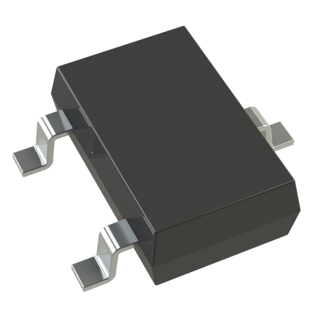
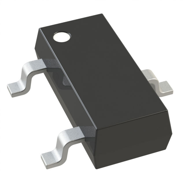
TRANS PREBIAS PNP 50V SOT23-3
- In stock 0

Information of Device Model NSVMMUN2113LT3G
1. Basic Product Information
1.1 Product Series
Digital Transistors (BRT) - PNP Transistors with Monolithic Bias Resistor Network
1.2 Core Function
Integrates a single PNP transistor with a monolithic bias resistor network (R1 = 47 kΩ, R2 = 47 kΩ), replacing discrete transistors and external bias resistors to simplify circuit design, reduce board space, and lower component count.
1.3 Key Compliance & Qualifications
- AEC-Q101 Qualified and PPAP Capable, suitable for automotive and other applications requiring unique site and control change requirements.
- Pb-Free, Halogen Free/BFR Free, and RoHS Compliant.
1.4 Discontinuation Status
Marked as DISCONTINUED; not recommended for new designs. For the latest information or alternative solutions, contact an onsemi representative or visit www.onsemi.com.
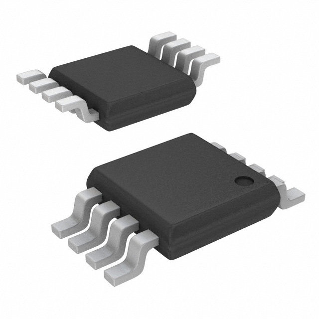
2. Ordering & Packaging Information
| Parameter | Details |
|---|---|
| Part Marking | A6C |
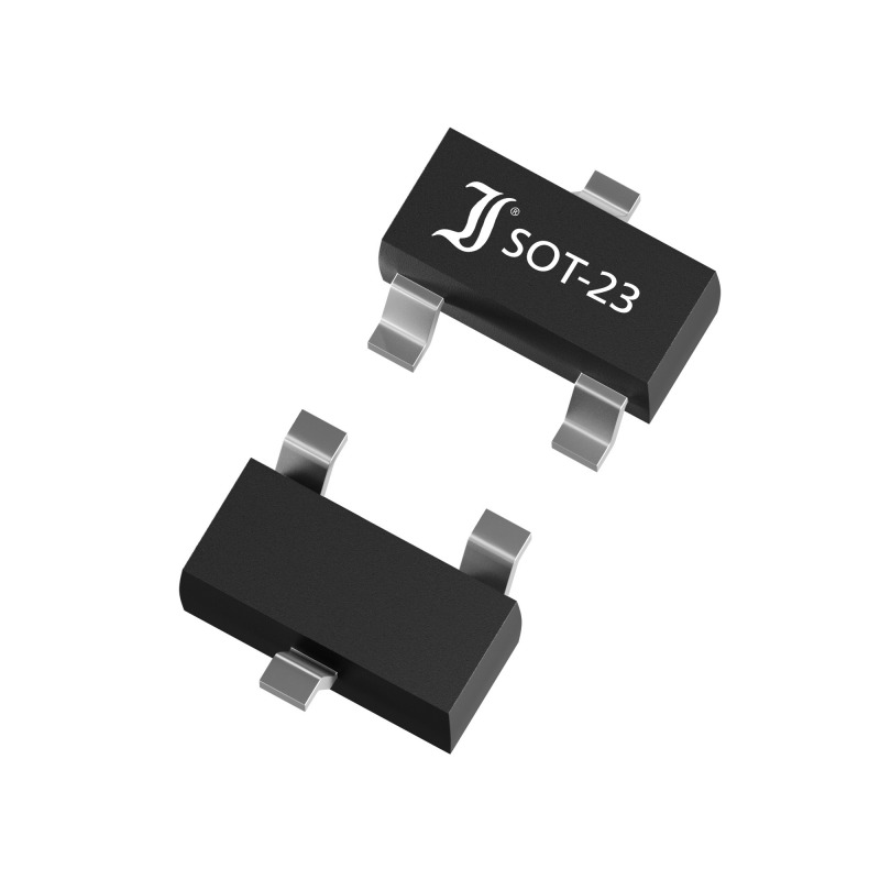
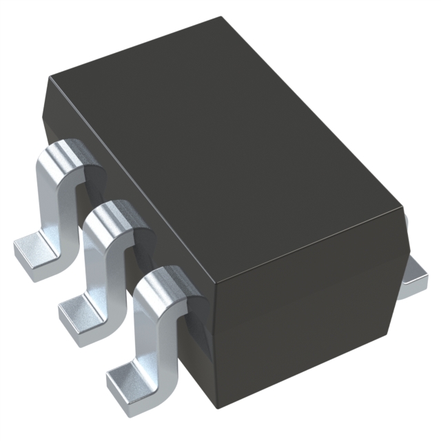
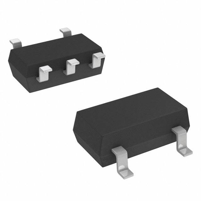
| Package Type | SOT−23 (Pb−Free), CASE 318 STYLE 6 |
| Shipping Quantity | 10,000 pieces per Tape & Reel |
| Tape & Reel Specifications | Refer to onsemi’s Tape and Reel Packaging Specifications Brochure (BRD8011/D) for details on part orientation, tape sizes, and related requirements. |
| Label/Marking Notes | Pb-Free package; marking includes specific device code ("A6C") and date code. A microdot may be present as a Pb-Free indicator (location may vary). |
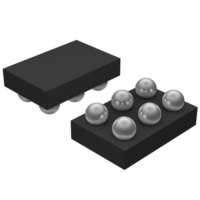
3. Pin Configuration (SOT−23 STYLE 6)
| Pin Number | Function | Description |
|---|---|---|
| PIN 1 | BASE (INPUT) | Connected to the monolithic bias resistor network (R1, R2). |
| PIN 2 | EMITTER (GROUND) | Ground connection terminal. |
| PIN 3 | COLLECTOR (OUTPUT) | Output terminal for the transistor. |
4. Maximum Ratings (TA = 25°C)
| Rating | Symbol | Maximum Value | Unit |
|---|---|---|---|
| Collector−Base Voltage | VCBO | 50 | Vdc |
| Collector−Emitter Voltage | VCEO | 50 | Vdc |
| Continuous Collector Current | IC | 100 | mAdc |
| Input Forward Voltage | VIN(fwd) | 40 | Vdc |
| Input Reverse Voltage | VIN(rev) | 10 | Vdc |
| Notes | Stresses exceeding these ratings may damage the device. Device functionality is not guaranteed if limits are violated, and reliability may be impaired. |
5. Thermal Characteristics (SOT−23 Package, TA = 25°C Unless Noted)
| Characteristic | Symbol | Value (Note 2) | Value (Note 3) | Unit |
|---|---|---|---|---|
| Total Device Dissipation | PD | 246 | 400 | mW |
| Derate Above 25°C | - | 2.0 | 3.2 | mW/°C |
| Thermal Resistance (Junction to Ambient) | RJA | 508 | 311 | °C/W |
| Thermal Resistance (Junction to Lead) | RJL | 174 | 208 | °C/W |
| Junction and Storage Temperature Range | TJ, Tstg | -55 to +150 | -55 to +150 | °C |
| Notes | 2. Test condition: FR−4 @ Minimum Pad. 3. Test condition: FR−4 @ 1.0 x 1.0 Inch Pad. |
6. Electrical Characteristics (TA = 25°C Unless Noted)
| Characteristic | Symbol | Minimum | Typical | Maximum | Unit | Test Conditions |
|---|---|---|---|---|---|---|
| OFF CHARACTERISTICS | ||||||
| Collector-Base Cutoff Current | - | - | - | 100 | nAdc | VCB = 50V, IE = 0 |
| Collector-Emitter Cutoff Current | ICEO | - | - | 500 | nAdc | VCE = 50V, IB = 0 |
| Emitter-Base Cutoff Current | - | - | - | 0.1 | mAdc | VEB = 6.0V, IC = 0 |
| Collector-Base Breakdown Voltage | V(BR)CBO | 50 | - | - | Vdc | IC = 10μA, IE = 0 |
| Collector-Emitter Breakdown Voltage | V(BR)CEO | 50 | - | - | Vdc | IC = 2.0mA, IB = 0 (Note 6) |
| ON CHARACTERISTICS | ||||||
| DC Current Gain | hFE | - | 140 | - | - | IC = 5.0mA, VCE = 10V (Note 6) |
| Collector-Emitter Saturation Voltage | VCE(sat) | - | - | 0.25 | Vdc | IC = 10mA, IB = 0.3mA (Note 6) |
| Input Voltage (Off) | Vi(off) | - | - | 0.8 | Vdc | - |
| Input Voltage (On) | Vi(on) | 1.6 | 3.0 | - | Vdc | VCE = 0.3V, IC = 2.0mA |
| Output Voltage (On) | VOL | - | - | 0.2 | Vdc | VCC = 5.0V, VB = 3.5V, RL = 1.0kΩ |
| Output Voltage (Off) | VOH | 4.9 | - | - | Vdc | VCC = 5.0V, VB = 0.5V, RL = 1.0kΩ |
| Input Resistor (R1) | R1 | 32.9 | 47 | 61.1 | kΩ | - |
| Input Resistor Ratio (R2/R1) | - | 0.8 | 1.0 | 1.2 | - | - |
| Notes | 6. Pulsed Condition: Pulse Width = 300 msec, Duty Cycle ≤ 2%. Product performance may vary if operated outside the specified test conditions. |
7. Package Mechanical Dimensions (SOT−23, CASE 318 ISSUE AU, Unit: mm)
| Dimension | Minimum | Nominal | Maximum |
|---|---|---|---|
| A (Package Height) | 0.89 | 1.00 | 1.11 |
| A1 (Lead Protrusion Below Seating Plane) | 0.01 | 0.06 | 0.10 |
| b (Lead Width) | 0.37 | 0.44 | 0.50 |
| C (Lead Thickness) | 0.08 | 0.14 | 0.20 |
| D (Package Length) | 2.80 | 2.90 | 3.04 |
| E (Package Width) | 1.20 | 1.30 | 1.40 |
| e (Lead Pitch) | 1.78 | 1.90 | 2.04 |
| L (Lead Length) | 0.30 | 0.43 | 0.55 |
| L1 (Lead Length from Package Body) | 0.35 | 0.54 | 0.69 |
| HE (Overall Height) | 2.10 | 2.40 | 2.64 |
| Notes | 1. Dimensions D and E do not include mold flash, protrusions, or gate burrs. 2. Maximum lead thickness (C) includes lead finish; minimum value refers to base material thickness. 3. Dimensioning and tolerancing conform to relevant standards. |
8. Recommended Mounting & Soldering
8.1 Mounting Footprint
Refer to the generic recommended mounting footprint for SOT−23 packages provided in the onsemi data sheet. For precise footprint design, follow the guidelines in the onsemi Soldering and Mounting Techniques Reference Manual (SOLDERRM/D).
8.2 Soldering Notes
- The device is Pb-Free; use compatible soldering processes and materials.
- For detailed soldering parameters (temperature profiles, dwell times, etc.), refer to SOLDERRM/D.
- Ensure adequate PCB pad size per thermal characteristic requirements (Minimum Pad or 1.0 x 1.0 Inch Pad) to optimize heat dissipation.
9. Typical Characteristics (Refer to Data Sheet Figures)
Key typical performance curves (available in the original data sheet) include:
- Figure 2: VCE(sat) vs. IC (Collector-Emitter Saturation Voltage vs. Collector Current)
- Figure 3: DC Current Gain (hFE) vs. IC at different temperatures (-25°C, 25°C, 75°C)
- Figure 4: Output Capacitance (Cob) vs. Reverse Voltage (VR)
- Figure 5: Output Current (IC) vs. Input Voltage (Vin)
- Figure 6: Input Voltage (Vin) vs. Output Current (IC)
10. Handling & Additional Information
10.1 Handling Precautions
- Avoid exceeding maximum ratings to prevent device damage.
- Store and handle the device within the specified junction and storage temperature range (-55°C to +150°C).
- For Pb-Free soldering best practices, refer to SOLDERRM/D.
Purchase
No need to register to order from JMBom Electronics, but signing in lets you track your order like a pro. Give it a try for a smoother shopping ride.
Means
Easy peasy! Pay your way with PayPal, Credit Card, or wire transfer in USD. We've got you covered.
RFQ(Request for Quotations)
Get the freshest prices and stock updates by asking for a quote! Our sales team will shoot you an email within a day. It's that simple.
IMPORTANT NOTICE
1. Look out for your order details in your inbox! (If it's missing, check the spam folder just in case.)
2. Our sales manager will double-check the order and keep you posted on any price or stock changes. No worries, we've got you covered.

Shipping Rate
We ship orders once a day around 5 p.m., except Sunday. Once shipped, the estimated delivery time depends on the courier company you choose, usually 5-7 working days.

Shipping Methods
We provide DHL, FedEx, UPS, EMS, SF Express, and Registered Air Mail international shipping.


Payment
You can pay the orders on the website directly or pay by wire transfer offline. We support: Paypal、VISA、Credit Card.


onsemi
onsemi
onsemi
onsemi
onsemi
onsemi
onsemi
onsemi
onsemi
onsemi
onsemi

onsemi