CP2108 USB to Quad UART Bridge Controller
Catalog
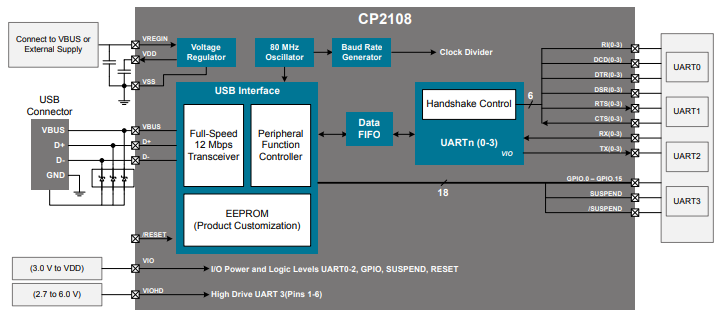
CP2108 – Key Features and ApplicationsFeature List and Ordering InformationSystem OverviewElectrical SpecificationsUART, GPIO, and Suspend I/O Electrical CharacteristicsGPIO Electrical CharacteristicsVoltage Regulator Electrical CharacteristicsUSB Transceiver Electrical CharacteristicsAbsolute Maximum RatingsThermal ConditionsPin DefinitionsCP2108 QFN64 Pin DefinitionsRelated ArticlesThe CP2108 is a fully integrated USB-to-Quad UART Bridge Controller that offers an easy way to upgrade RS-232 or RS-485 designs to USB while using very few components and minimal PCB space.
This device features a USB 2.0 full-speed controller, USB transceiver, oscillator, EEPROM, and four asynchronous UART interfaces with full modem control signals, all in a compact 9 mm × 9 mm, 64-pin QFN package.
The built-in EEPROM allows customization of the USB Vendor ID (VID), Product ID (PID), product description string, power descriptor, device release number, interface strings, serial number, as well as modem and GPIO settings to match specific application needs. All configuration can be done through a user-friendly, GUI-based tool.
By removing the need for complex firmware or driver development, the CP2108 makes it possible to establish USB connectivity quickly and with minimal development effort.
CP2108 – Key Features and Applications
The CP2108 is designed for versatility and is well-suited to a wide variety of applications, such as:
Key Features
- No firmware development required
- Intuitive, GUI-based configuration tool
- Built-in USB transceiver (no need for external resistors)
- Integrated clock (eliminates the need for an external crystal)
- Fully compatible with USB 2.0 full-speed
- Four independent UART channels
- 16 configurable GPIO pins
- Royalty-free Virtual COM Port (VCP) drivers
Typical Applications
- Instrumentation
- Industrial automation and control
- Server systems
- Point-of-Sale (POS) devices
Feature List and Ordering Information
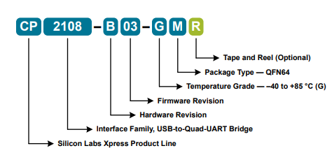
CP2108 Part Numbering
Features of the CP2108
- Single-chip USB-to-Quad UART data transfer solution
- Four fully independent UART interfaces
- Built-in USB transceiver (no external resistor needed)
- Integrated clock (no external crystal required)
- On-chip programmable EEPROM for storing custom product information
- Power-on reset circuit integrated on-chip
- On-chip 3.3 V voltage regulator output
- USB peripheral function controller
- Compliant with USB 2.0 specification; supports full-speed (12 Mbps) operation
- USB suspend modes supported through SUSPEND pins
- Virtual COM Port (VCP) drivers included
- Compatible with existing PC applications that use COM ports
- Royalty-free driver distribution license
- Cross-platform support for Windows, macOS, and Linux
- Supply voltage options: Self-powered: 3.0 V to 3.6 V USB bus-powered: 4.0 V to 5.5 V VIO voltage: 3.0 V to VDD VIOHD voltage: 2.7 V to 6 V
UART Interface Features
Each UART interface includes the following capabilities:
- Hardware flow control support (RTS/CTS)
- Full set of modem control signals
- Supported data formats: Data bits: 5, 6, 7, or 8 Stop bits: 1, 1.5, or 2 Parity: odd, even, mark, space, or none
- Baud rates from 300 bps up to 2 Mbps
- UART 3 (pins 1–6) supports connections to devices operating up to 6 V
GPIO Interface Features
- 16 configurable GPIO pins
- Suspend pin support
- Can function as inputs, open-drain outputs, or push-pull outputs
- Four configurable clock outputs for driving external devices
- RS-485 bus transceiver control
- LED toggle capability on transmit and receive
Package Options
- RoHS-compliant 64-pin QFN package (9 × 9 mm)
Operating Temperature Range
- –40 °C to +85 °C
Ordering Information
- Part Number: CP2108-B03-GM
System Overview
The CP2108 is a fully integrated USB-to-Quad UART Bridge Controller that offers a straightforward way to upgrade RS-232/RS-485 designs to USB while requiring very few external components and minimal PCB space.
It incorporates a USB 2.0 full-speed function controller, USB transceiver, oscillator, EEPROM, and four asynchronous UART interfaces with full modem control signals, all housed in a compact 9 × 9 mm QFN-64 package (also known as “MLF” or “MLP”).
The built-in EEPROM can be customized to store parameters such as USB Vendor ID (VID), Product ID (PID), product description string, power descriptor, device release number, interface strings, serial number, as well as modem and GPIO configurations. Programming is performed directly via USB, making it easy to integrate into manufacturing and test workflows.
Silicon Labs provides royalty-free Virtual COM Port (VCP) drivers, which allow a CP2108-based device to appear as four independent COM ports in PC applications. The CP2108 UART interfaces fully support RS-232/RS-485 control and handshaking signals, eliminating the need to change existing firmware. In addition, the device includes 16 user-configurable GPIO pins that can be assigned for system status or control functions.
Electrical Specifications
Electrical Characteristics
All electrical parameters provided in the following tables are valid under the conditions defined in 3.1.1 Recommended Operating Conditions, unless otherwise noted.
Recommended Operating Conditions
VDD = 3.0 to 3.6 V, TA = –40 to +85 °C unless otherwise specified.
Recommended Operating Conditions¹
| Parameter | Symbol | Test Condition | Min | Typ | Max | Unit |
|---|---|---|---|---|---|---|
| Operating Supply Voltage | VDD | — | 3.0 | — | 3.6 | V |
| Operating Supply Voltage | VREGIN² | — | 4.0 | — | 5.5 | V |
| Operating Supply Voltage | VIO | — | 3.0 | — | VDD | V |
| Operating Supply Voltage | VIOHD | — | 2.7 | — | 6.0 | V |
| Supply Current — Normal³ | IDD | — | — | 56 | — | mA |
| Supply Current — Suspended³ | IDD | Bus Powered | — | 460 | — | µA |
| Self Powered | — | 330 | — | µA | ||
| Supply Current — USB Pull-up⁴ | IPU | — | — | 200 | 228 | µA |
| Operating Ambient Temperature | TA | — | -40 | — | 85 | °C |
| Operating Junction Temperature | TJ | — | -40 | — | 105 | °C |
Notes:
- All voltages are referenced to VSS.
- Applies only when using the on-chip regulator. If the regulator is not used, VREGIN and VDD must be tied together externally, and VREGIN may equal VDD.
- If the device is connected to the USB bus, add the USB pull-up current to the supply current to determine total current requirements.
- USB pull-up supply current values are derived from USB specification calculations.
UART, GPIO, and Suspend I/O Electrical Characteristics
Conditions: VDD = 3.0–3.6 V, VIO = 1.8 V to VDD, VIOHD = 2.7 V to 6.0 V, TA = –40 to +85 °C (unless otherwise specified).
UART, GPIO, and Suspend I/O Characteristics
| Parameter | Symbol | Test Condition | Min | Typ | Max | Unit |
|---|---|---|---|---|---|---|
| Output High Voltage (all pins except High-Drive UART3, pins 1–6) | VOH | — | VIO – 0.7 | — | — | V |
| Output High Voltage (High-Drive UART3, pins 1–6) | VOH | — | VIOHD – 0.7 | — | — | V |
| Output Low Voltage (all pins except High-Drive pins 1–6) | VOL | IOL = 3 mA (Low Drive) | — | — | 0.6 | V |
| Output Low Voltage (High-Drive pins 1–6) | VOL | IOL = 12.5 mA (High Drive) | — | — | 0.6 | V |
| Input High Voltage | VIH | 3.0 ≤ VIO ≤ 3.6 | VIO – 0.6 | — | — | V |
| Input Low Voltage | VIL | — | — | 0.6 | V | |
| Weak Pull-up Current (VIN = 0 V) | IPU | VIO = 3.6 V | -30 | -20 | -10 | µA |
| Weak Pull-up Current (UART3, pins 1–6) | IPU | VIOHD = 2.7 V | -15 | -10 | -5 | µA |
| VIOHD = 6.0 V | -30 | -20 | -10 | µA |
GPIO Electrical Characteristics
Conditions: TA = –40 to +85 °C unless otherwise specified.
GPIO Output Specifications
| Parameter | Symbol | Test Condition | Min | Typ | Max | Unit |
|---|---|---|---|---|---|---|
| RS-485 Active Time After Stop Bit | tACTIVE | — | 1 | — | bit time¹ | |
| TX Toggle Rate | fTXTOG | — | — | 15 | — | Hz |
| RX Toggle Rate | fRXTOG | — | — | 15 | — | Hz |
| Clock Output Rate | fCLOCK | ~158k | — | 20M | Hz |
Note:
- Bit time is defined as 1 / baud rate.
Reset Electrical Characteristics
Conditions: TA = –40 to +85 °C unless otherwise specified.
Reset Specifications
| Parameter | Symbol | Test Condition | Min | Typ | Max | Unit |
|---|---|---|---|---|---|---|
| Power-On Reset (POR) Threshold | VPOR | Rising voltage on VDD | — | 1.4 | — | V |
| Falling voltage on VDD | 0.8 | 1.0 | 1.3 | V | ||
| VDD Ramp Time | tRMP | Time for VDD ≥ 3.0 V | 10 | — | 3000 | µs |
| /RESET Input High Voltage | VIHRESET | 3.0 ≤ VIO ≤ 3.6 | VIO – 0.6 | — | — | V |
| /RESET Input Low Voltage | VILRESET | — | — | 0.6 | V | |
| /RESET Low Time to Trigger Reset | tRSTL | — | 50 | — | — | ns |
Voltage Regulator Electrical Characteristics
Conditions: TA = –40 to +85 °C unless otherwise specified.
Table 3.5. Voltage Regulator Specifications
| Parameter | Symbol | Test Condition | Min | Typ | Max | Unit |
|---|---|---|---|---|---|---|
| Output Voltage (at VDD pin) | VDDOUT | — | 3.15 | 3.3 | 3.4 | V |
| Output Current (at VDD pin)¹ | IDDOUT | — | — | 150 | mA | |
| Output Load Regulation | VDDLR | — | 0.1 | 1.0 | mV/mA | |
| Output Capacitance | CVDD | — | 1 | — | 10 | µF |
Note:
- The value listed is the maximum total current the regulator can provide. Any current consumed internally by the CP2108 reduces the amount available to power external devices through VDD.
USB Transceiver Electrical Characteristics
Conditions: TA = –40 to +85 °C unless otherwise specified.
USB Transceiver Specifications
| Parameter | Symbol | Test Condition | Min | Typ | Max | Unit |
|---|---|---|---|---|---|---|
| Valid Supply Range (USB compliance) | VDD | — | 3.0 | — | 3.6 | V |
| VBUS Pull-Down Leakage Current | IVBUSL | VBUS = 5 V, VIO = 3.3 V | — | 10 | — | µA |
| VBUS Detection Input Threshold | VVBUSTH | 3.0 ≤ VIO ≤ 3.6 | VIO – 0.6 | — | — | V |
Transmitter Characteristics
| Parameter | Symbol | Test Condition | Min | Typ | Max | Unit |
|---|---|---|---|---|---|---|
| Output High Voltage | VOH | — | 2.8 | — | — | V |
| Output Low Voltage | VOL | — | — | 0.8 | V | |
| Output Crossover Point | VCRS | — | 1.3 | — | 2.0 | V |
| Output Impedance | ZDRV | Driving High | — | 38 | — | Ω |
| Driving Low | — | 38 | — | Ω | ||
| Pull-up Resistance | RPU | Full-Speed (D+), Low-Speed (D–) | 1.425 | 1.5 | 1.575 | kΩ |
| Output Rise Time | TR | Low-Speed | 75 | — | 300 | ns |
| Full-Speed | 4 | — | 20 | ns | ||
| Output Fall Time | TF | Low-Speed | 75 | — | 300 | ns |
| Full-Speed | 4 | — | 20 | ns |
Receiver Characteristics
| Parameter | Symbol | Test Condition | Min | Typ | Max | Unit |
|---|---|---|---|---|---|---|
| Differential Input Sensitivity | VDI | (D+) – (D–) | 0.2 | — | ||
| Differential Input Common Mode Range | VCM | — | 0.8 | — | 2.5 | V |
| Input Leakage Current | IL | Pull-ups Disabled | — | <1.0 | — | µA |
Note:
Refer to the official USB Specification for timing diagrams and symbol definitions.
Absolute Maximum Ratings
Caution: Exceeding the limits listed below may cause permanent damage to the device. These values represent stress ratings only; functional operation at these or higher conditions is not guaranteed. Prolonged exposure to maximum ratings may affect device reliability.
Absolute Maximum Ratings
| Parameter | Symbol | Test Condition | Min | Max | Unit |
|---|---|---|---|---|---|
| Ambient Temperature Under Bias | TBIAS | — | -55 | 125 | °C |
| Storage Temperature | TSTG | — | -65 | 150 | °C |
| Voltage on VDD | VDD | — | VSS – 0.3 | 4.2 | V |
| Voltage on VREGIN | VREGIN | — | VSS – 0.3 | 6.0 | V |
| Voltage on VBUS | VBUS | VIO ≥ 3.3 V | VSS – 0.3 | 5.8 | V |
| VIO < 3.3 V | VSS – 0.3 | VIO + 2.5 | V | ||
| Voltage on VIO | VIO | — | VSS – 0.3 | 4.2 | V |
| Voltage on VIOHD | VIOHD | — | VSS – 0.3 | 6.5 | V |
| Voltage on /RESET | VIN | VIO ≥ 3.3 V | VSS – 0.3 | 5.8 | V |
| VIO < 3.3 V | VSS – 0.3 | VIO + 2.5 | V | ||
| Voltage on GPIO or UART pins | VIN | GPIO/UART pins except 1–6 | VSS – 0.3 | VIO + 0.3 | V |
| UART pins 1–6 | VSSHD – 0.3 | VIOHD + 0.3 | V | ||
| Voltage on D+ or D– | VIN | VIO ≥ 3.3 V | VSS – 0.3 | 5.8 | V |
| VIO < 3.3 V | VSS – 0.3 | VIO + 2.5 | V | ||
| Total Current Sunk into Supply Pins | ISUPP | VDD, VREGIN, VIO, VIOHD | — | 400 | mA |
| Total Current Sourced from Ground Pins | IVSS | — | 400 | — | mA |
| Current Sourced or Sunk by Any I/O Pin | IPIO | UART, GPIO, Suspend I/O, /RESET (except UART 3 pins 1–6) | -100 | 100 | mA |
| UART 3 pins 1–6 | -300 | 300 | mA | ||
| Current Injected on Any I/O Pin | IINJ | UART, GPIO, Suspend I/O, /RESET (except UART 3 pins 1–6) | -100 | 100 | mA |
| UART 3 pins 1–6 | -300 | 300 | mA | ||
| Total Injected Current on I/O Pins | ∑IINJ | Sum of all I/O and /RESET pins | -400 | 400 | mA |
| Power Dissipation (TA = 85 °C) | PD | — | — | 800 | mW |
Note:
- VSS and VSSHD provide separate return paths for device supplies but are not electrically isolated. Both must always be connected to the same potential on the PCB.
Thermal Conditions
Thermal Characteristics
| Parameter | Symbol | Test Condition | Min | Typ | Max | Unit |
|---|---|---|---|---|---|---|
| Thermal Resistance | θJA | — | — | 25 | — | °C/W |
Note:
- Thermal resistance assumes a multi-layer PCB with any exposed pad properly soldered to the PCB pad.
Throughput and Flow Control
The throughput values in the following table are typical results obtained from bench testing and are intended as a guideline for expected performance. Actual throughput may vary depending on factors such as PC system performance and USB bus load. Each column shows typical throughput when using 1, 2, 3, or all 4 UART interfaces at the specified baud rate.
Guidelines:
- Hardware flow control is not required if all CP2108 interfaces are configured at 230,400 bps or lower.
- For baud rates above 230,400 bps, hardware flow control should be used to ensure complete data reception across the UART.
- Sending data simultaneously on multiple interfaces reduces the effective throughput for each interface.
- UART 3 typically achieves lower throughput than UARTs 0–2. When configuring interfaces with different baud rates, the interface with the lowest baud rate should be assigned to UART 3. Throughput on UART 3 is 5%–20% slower than the other UARTs.
- At baud rates above 230,400 bps, the performance of UART 3 degrades significantly compared to other interfaces.
Typical Throughput for UART Interfaces at Different Baud Rates
| Set Baud Rate | 230,400 bps | 460,800 bps | 921,600 bps | 2 Mbps |
|---|---|---|---|---|
| 1 UART in operation | 196,900 | 387,200 | 694,200 | 760,000 |
| 2 UARTs in operation | 200,400 | 381,600 | 463,700 | 537,400 |
| 3 UARTs in operation | 200,300 | 259,800 | 314,800 | 388,000 |
| 4 UARTs in operation | 180,300 | 208,900 | 234,000 | 288,200 |
Pin Definitions
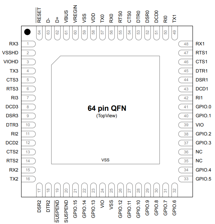
CP2108 Pin Definitions
CP2108 QFN64 Pin Definitions
| Pin Name | Type | Pin Number | Primary Function | Alternate Function |
|---|---|---|---|---|
| VSS | Ground | 25, 59 | Device Ground | — |
| VSSHD | Ground (High Drive) | 2 | High-Drive Device Ground (for UART 3 pins 1–6) | Connect to device ground |
| VDD | Power (Core) | 58 | Core Power Supply Input | Voltage Regulator Output |
| VIO | Power (I/O, Non-High Drive) | 24, 39 | Non-High Drive I/O Supply Input | — |
| VIOHD | Power (I/O, High Drive) | 3 | High-Drive I/O Supply Input | — |
| VREGIN | Power (Regulator) | 60 | Input to the on-chip voltage regulator | — |
| RESET | Active-Low Reset | 64 | Device Reset (Open-drain output from internal POR or VDD monitor). Can also be driven externally to reset the system. | — |
| D– | USB Data- | 63 | USB D– signal | — |
| D+ | USB Data+ | 62 | USB D+ signal | — |
| VBUS | USB Bus Sense | 61 | Sense input. Connect to the VBUS signal of a USB network | — |
| TX0 | Digital Output | 57 | UART 0 Transmit (TX) | — |
| RX0 | Digital Input | 56 | UART 0 Receive (RX) | — |
| RTS0 | Digital Output | 55 | UART 0 Ready to Send. Indicates the UART is ready to receive data | — |
| CTS0 | Digital Input | 54 | UART 0 Clear to Send. Indicates the modem is ready to send data to the UART | — |
| DTR0 | Digital Output | 53 | UART 0 Data Terminal Ready. Informs the modem that the UART is ready to establish a communication link | — |
| DSR0 | Digital Input | 52 | UART 0 Data Set Ready. Indicates the modem is ready to establish a link with the UART | — |
| DCD0 | Digital Input | 51 | UART 0 Data Carrier Detect. Indicates the modem has detected a data carrier | — |
| RI0 | Digital Input | 50 | UART 0 Ring Indicator. Indicates that a telephone ringing signal has been detected | — |
| TX1 | Digital Output | 49 | UART 1 Transmit (TX) | — |
| RX1 | Digital Input | 48 | UART 1 Receive (RX) | — |
| RTS1 | Digital Output | 47 | UART 1 Ready to Send | — |
| CTS1 | Digital Input | 46 | UART 1 Clear to Send | — |
Related Articles
How to Check Resistance Using a Digital Multimeter
Capacitance Basics: Grasp the Concept and Use the Formula
Motor Load, Wiring and Breaker Specifications for Efficient Operation

Christopher Anderson
Christopher Anderson has a Ph.D. in electrical engineering, focusing on power electronics. He’s been a Senior member of the IEEE Power Electronics Society since 2021. Right now, he works with the KPR Institute of Engineering and Technology in the U.S. He also writes detailed, top-notch articles about power electronics for business-to-business electronics platforms.
Subscribe to JMBom Electronics !