


TC4420/TC4429 High-Speed MOSFET Drivers
Catalog
OverviewKey FeaturesTypical ApplicationsPackage TypesFunctional Block DiagramElectrical SpecificationsPin ConfigurationConclusionFrequently Ask QuestionsRelated ArticlesOverview
The TC4420 and TC4429 are high-performance, single-output MOSFET drivers capable of delivering 6A peak current. The TC4429 provides inverting operation (pin-compatible with the TC429), while the TC4420 offers non-inverting operation. Both are built using CMOS technology, delivering lower power consumption and improved efficiency compared to bipolar drivers.
TC4420/TC4429
These devices feature TTL/CMOS-compatible inputs that can handle voltages up to VDD + 0.3V or down to –5V without risk of malfunction or damage. This design removes the need for external level-shifting components, reducing both cost and board space. With rail-to-rail output capability, they deliver a wide voltage swing and maintain solid drive margins, even during power-up or power-down transitions.
The TC4420/TC4429 achieve a typical propagation delay of just 55 ns, with rise and fall times of about 25 ns when driving a 2500 pF load, across the full supply voltage range.
Unlike many other drivers, these devices are virtually immune to latch-up. By replacing three or more discrete parts, they help minimize PCB footprint, lower component count, and enhance overall system reliability.
Key Features
- Latch-Up Protection: Can tolerate over 1.5A reverse output current.
- Robust Logic Inputs: Withstands negative voltage swings up to –5V.
- ESD Protection: Up to 4 kV.
- Balanced Rise and Fall Times: Typically 25 ns with a 2500 pF load.
- High Peak Output Current: 6A.
- Wide Supply Voltage Range: Operates from 4.5V to 18V.
- Strong Capacitive Load Drive: Can handle up to 10,000 pF.
- Fast Propagation Delay: Typical 55 ns.
- CMOS/TTL-Compatible Inputs for flexible interfacing.
- Low Supply Current: Typically 450 µA with logic “1” input.
- Low Output Impedance: 2.5 Ω.
- Rail-to-Rail Output: Voltage swing within 25 mV of ground or VDD.
- Compact Packages: Available in 8-pin SOIC and 8-pin 6x5 DFN.
Typical Applications
- Switch-Mode Power Supplies (SMPS)
- Motor Control Circuits
- Pulse Transformer Drivers
- Class D Switching Amplifiers
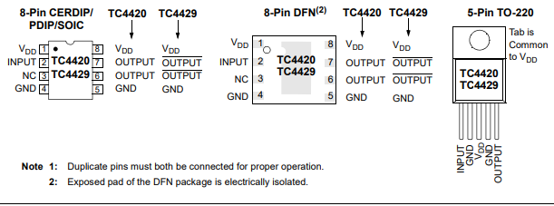
Package Types
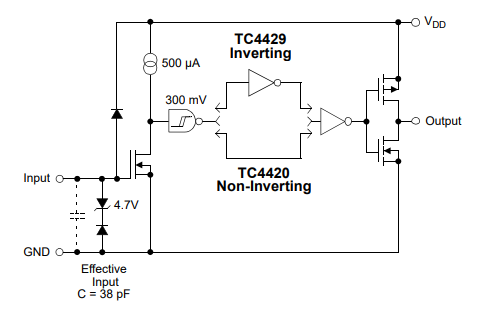
Functional Block Diagram
Electrical Specifications
Unless otherwise specified: TA = +25°C, 4.5V ≤ VDD ≤ 18V
| Parameter | Symbol | Min | Typ | Max | Units | Conditions |
|---|---|---|---|---|---|---|
| Input | ||||||
| High-Level Input Voltage | VIH | 1.8 | 2.4 | — | V | Logic “1” |
| Low-Level Input Voltage | VIL | — | 0.8 | 1.3 | V | Logic “0” |
| Input Voltage Range | VIN | –5 | — | VDD + 0.3 | V | — |
| Input Current | IIN | –10 | — | 10 | µA | 0V ≤ VIN ≤ VDD |
| Output | ||||||
| High-Level Output Voltage | VOH | VDD – 0.025 | — | — | V | DC test |
| Low-Level Output Voltage | VOL | — | — | 0.025 | V | DC test |
| High Output Resistance | ROH | 2.1 | — | 2.8 | Ω | IOUT = 10 mA, VDD = 18V |
| Low Output Resistance | ROL | 1.5 | — | 2.5 | Ω | IOUT = 10 mA, VDD = 18V |
| Peak Output Current | IPK | — | 6.0 | — | A | VDD = 18V |
| Latch-Up Protection | ||||||
| Reverse Current Tolerance | IREV | — | >1.5 | — | A | Duty cycle ≤ 2%, t ≤ 300 µs |
| Switching Times (Note 1) | ||||||
| Rise Time | tR | — | 25 | 35 | ns | CL = 2500 pF |
| Fall Time | tF | — | 25 | 35 | ns | CL = 2500 pF |
| Delay Time (Low to High) | tD1 | — | 55 | 75 | ns | — |
| Delay Time (High to Low) | tD2 | — | 55 | 75 | ns | — |
| Power Supply | ||||||
| Supply Current, VIN = 3V | IS | — | 0.45 | 1.5 | mA | — |
| Supply Current, VIN = 0V | IS | — | 55 | 150 | µA | — |
| Operating Supply Voltage | VDD | 4.5 | — | 18 | V | — |
Notes:
- Switching times are guaranteed by design.
- Package power dissipation depends on the copper pad area on the PCB.
Pin Configuration
| Pin No. (8-Pin CERDIP/PDIP/SOIC) | Pin No. (8-Pin DFN) | Pin No. (5-Pin TO-220) | Symbol | Description |
|---|---|---|---|---|
| 1 | 1 | — | VDD | Supply voltage input, 4.5V to 18V |
| 2 | 2 | 1 | INPUT | Control input, TTL/CMOS-compatible |
| 3 | 3 | — | NC | No connection |
| 4 | 4 | 2 | GND | Ground |
| 5 | 5 | 4 | GND | Ground |
| 6 | 6 | 5 | OUTPUT | CMOS push-pull output |
| 7 | 7 | — | OUTPUT | CMOS push-pull output |
| 8 | 8 | 3 | VDD | Supply voltage input, 4.5V to 18V |
| — | PAD | — | NC | Exposed metal pad (no connection) |
| — | — | TAB | VDD | Metal tab connected to VDD |
Supply Input (VDD)
The VDD pin provides the bias voltage for the MOSFET driver and supports a range of 4.5V to 18V relative to the ground pins. It is recommended to bypass VDD to ground using a local ceramic capacitor. The capacitor value should be selected according to the capacitive load being driven, with a minimum of 1.0 µF suggested for stable operation.
Control Input
The input of the MOSFET driver is a high-impedance, TTL/CMOS-compatible pin. The TC4420/TC4429 includes an internal “speed-up” capacitor that reduces propagation delay. Because of this, input signals with slow rise or fall times should be avoided, as they can cause double-pulsing at the driver output.
CMOS Push-Pull Output
The MOSFET driver features a low-impedance, CMOS push-pull output capable of delivering peak currents up to 6.0A to drive capacitive loads. It can also tolerate peak reverse currents of up to 1.5A in either direction without damage.
Ground
The ground pins provide the return path for both the bias current and the high peak currents used to discharge the load capacitor. For optimal performance, connect the ground pins to a ground plane or use very short traces to the bias supply return.
Exposed Metal Pad (DFN Package)
The exposed metal pad on the 6x5 DFN package is not internally connected to any potential. It can be connected to a ground plane or other copper area on the PCB to help dissipate heat and improve thermal performance.
Switching Time Test Circuits
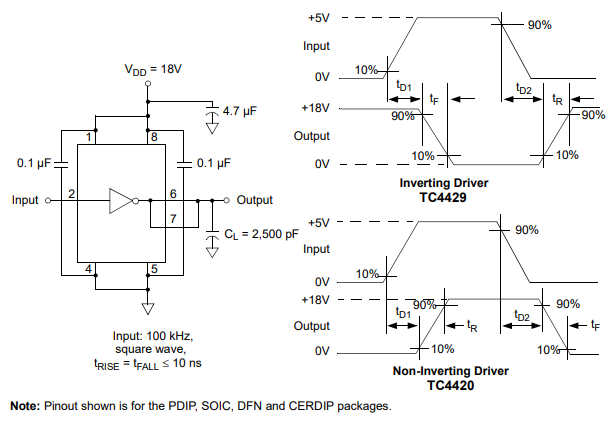
Switching Time Test Circuits
Conclusion
The TC4420/TC4429 are high-speed, CMOS-based MOSFET drivers that deliver reliable, high-current performance in compact packages. With robust latch-up protection, wide voltage range, fast switching, and strong capacitive load handling, they simplify circuit design, reduce component count, and enhance overall system efficiency and reliability across applications such as Class D amplifiers, motor control, and switch-mode power supplies.
Frequently Ask Questions
What is the TC4420?
The TC4420 is a high-speed, single-output, non-inverting MOSFET driver, ideal for Class D switching amplifiers. It’s built with CMOS technology, offering lower power consumption and greater efficiency compared to traditional bipolar drivers.
How does the TC4420 compare to other drivers?
The TC4420 (and TC4429) are virtually immune to latch-up, making them more reliable than many other drivers. They can replace three or more discrete components, saving PCB space, reducing part count, and improving overall system reliability.
Note: Duplicate pins must both be connected for proper operation, and the exposed pad on the DFN package is electrically isolated.
What are the common applications of the TC4420?
- The TC4420 can provide “SOURCE” current (via the internal P-channel MOSFET) to turn on an NPN bipolar transistor, with Ib limited by Rb and the driver.
- It can also provide “SINK” current (via the internal N-channel MOSFET) to turn on a PNP bipolar transistor.
Is the TC4420 suitable for high-frequency applications?
Yes. With a peak output current of up to 6A, the TC4420 is designed for high-performance operation in demanding, high-frequency applications, making it ideal for efficient power management and fast switching environments.
What is the output current of the TC4420?
The TC4420 is a high-current, non-inverting MOSFET driver capable of delivering peak currents up to 6A.
How does a MOSFET gate driver work?
To turn on a MOSFET or IGBT, a voltage must be applied to its gate relative to the source (or emitter). The driver makes the gate positive with respect to the source/emitter, allowing the device to conduct and switch efficiently.
Related Articles
Capacitance Basics: Grasp the Concept and Use the Formula
Motor Load, Wiring and Breaker Specifications for Efficient Operation
Band Reject Filters: Principles and Uses
ADXL343: High-Performance 3-Axis MEMS Accelerometer
TIS Series Industrial Power Supplies:Features and Options
Efficient Logic and Memory Implementation with FLEX 10K EABs

Amanda Miller
Amanda Miller is a senior electronics engineer with 6 years of experience. She focuses on studying resistors, transistors, and package design in detail. Her deep knowledge helps her bring innovation and high standards to the electronics industry.
Subscribe to JMBom Electronics !


