


Efficient Logic and Memory Implementation with FLEX 10K EABs
Catalog
General DescriptionFeaturesFLEX 10K Device Features Supply Voltages for FLEX 10K & FLEX 10KA DevicesFunctional DescriptionFLEX 10K Device Block DiagramConclusionRelated ArticlesGeneral Description
Altera’s FLEX 10K devices were the industry’s first embedded PLDs. Built on reconfigurable CMOS SRAM technology, the Flexible Logic Element MatriX (FLEX) architecture integrates all the features needed to implement standard gate array megafunctions. With capacities of up to 250,000 gates, the FLEX 10K family delivers the density, speed, and functionality to integrate complete systems—including multiple 32-bit buses—onto a single chip.
FLEX 10K EABs
Because FLEX 10K devices are reconfigurable, every unit can be fully tested before shipment. This eliminates the need for designers to create test vectors for fault coverage. In addition, engineers no longer have to maintain separate inventories of different ASIC versions; instead, FLEX 10K devices can be programmed directly on the board to provide the exact functionality required.
Table 6 presents FLEX 10K performance benchmarks for a range of common designs. These results were generated using Synopsys DesignWare or LPM functions. No special optimization techniques were needed—the functions were simply inferred or instantiated in Verilog HDL, VHDL, Altera Hardware Description Language (AHDL), or schematic-based design files.
Features
■ The world’s first family of embedded programmable logic devices (PLDs), enabling full System-on-a-Programmable-Chip (SOPC) integration.
– Embedded array for advanced megafunctions, such as high-efficiency memory and custom logic functions
– General-purpose logic array for standard logic operations
■ High density
– Offers from 10,000 up to 250,000 typical logic gates (see Tables 1 and 2)
– Provides up to 40,960 RAM bits; each embedded array block (EAB) contains 2,048 bits, all usable without reducing overall logic resources
■ System-level capabilities
– MultiVolt™ I/O interface compatibility
– 5.0-V tolerant input pins available in FLEX® 10KA devices
– Low power requirements (typically under 0.5 mA in standby mode for most models)
– FLEX 10K and FLEX 10KA devices comply with PCI Local Bus Specification, Revision 2.2, from the PCI Special Interest Group (PCI SIG)
– FLEX 10KA devices include an optional pull-up clamping diode, configurable per pin, for 3.3-V PCI compatibility
– Certain FLEX 10KA devices also support 5.0-V PCI buses with up to eight loads
– Integrated JTAG (Joint Test Action Group) boundary-scan test (BST) circuitry, fully IEEE Std. 1149.1-1990 compliant, provided without using any device logic
FLEX 10K Device Features
| Feature | EPF10K10 / EPF10K10A | EPF10K20 | EPF10K30 / EPF10K30A | EPF10K40 | EPF10K50 / EPF10K50V |
|---|---|---|---|---|---|
| Typical gates (logic + RAM) (1) | 10,000 | 20,000 | 30,000 | 40,000 | 50,000 |
| Maximum system gates | 31,000 | 63,000 | 69,000 | 93,000 | 116,000 |
| Logic elements (LEs) | 576 | 1,152 | 1,728 | 2,304 | 2,880 |
| Logic array blocks (LABs) | 72 | 144 | 216 | 288 | 360 |
| Embedded array blocks (EABs) | 3 | 6 | 6 | 8 | 10 |
| Total RAM bits | 6,144 | 12,288 | 12,288 | 16,384 | 20,480 |
| Maximum user I/O pins | 150 | 189 | 246 | 189 | 310 |
FLEX 10K Device Features
| Feature | EPF10K70 | EPF10K100 / EPF10K100A | EPF10K130V | EPF10K250A |
|---|---|---|---|---|
| Typical gates (logic + RAM) (1) | 70,000 | 100,000 | 130,000 | 250,000 |
| Maximum system gates | 118,000 | 158,000 | 211,000 | 310,000 |
| Logic elements (LEs) | 3,744 | 4,992 | 6,656 | 12,160 |
| Logic array blocks (LABs) | 468 | 624 | 832 | 1,520 |
| Embedded array blocks (EABs) | 9 | 12 | 16 | 20 |
| Total RAM bits | 18,432 | 24,576 | 32,768 | 40,960 |
| Maximum user I/O pins | 358 | 406 | 470 | 470 |
Note to Tables
(1) The integrated IEEE Std. 1149.1 JTAG circuitry contributes up to 31,250 additional gates beyond the listed typical or maximum system gate counts.
Additional Features
– Built on advanced semiconductor processes, supporting operation with either 3.3-V or 5.0-V supply voltage (see Table 3)
– In-circuit reconfigurability (ICR) through an external configuration device, intelligent controller, or JTAG interface
– ClockLock™ and ClockBoost™ options for minimizing clock delay/skew and enabling clock multiplication
– Integrated low-skew clock distribution networks
– Every device undergoes 100% functional testing, eliminating the need for user-supplied test vectors or scan chains
FLEX 10K Device Features
| Feature | EPF10K70 | EPF10K100 / EPF10K100A | EPF10K130V | EPF10K250A |
|---|---|---|---|---|
| Typical gates (logic + RAM) (1) | 70,000 | 100,000 | 130,000 | 250,000 |
| Maximum system gates | 118,000 | 158,000 | 211,000 | 310,000 |
| Logic elements (LEs) | 3,744 | 4,992 | 6,656 | 12,160 |
| Logic array blocks (LABs) | 468 | 624 | 832 | 1,520 |
| Embedded array blocks (EABs) | 9 | 12 | 16 | 20 |
| Total RAM bits | 18,432 | 24,576 | 32,768 | 40,960 |
| Maximum user I/O pins | 358 | 406 | 470 | 470 |
Supply Voltages for FLEX 10K & FLEX 10KA Devices
| 5.0-V Devices | 3.3-V Devices |
|---|---|
| EPF10K10 | EPF10K10A |
| EPF10K20 | EPF10K30A |
| EPF10K30 | EPF10K50V |
| EPF10K40 | EPF10K100A |
| EPF10K50 | EPF10K130V |
| EPF10K70 | EPF10K250A |
| EPF10K100 |
Flexible Interconnect
– FastTrack® Interconnect architecture provides continuous routing paths for consistent, low-delay signal connections
– Dedicated carry chains for arithmetic functions such as fast adders, counters, and comparators (automatically used by software tools and megafunctions)
– Dedicated cascade chains for high-speed, wide fan-in logic operations (automatically utilized by tools and megafunctions)
– Tri-state emulation for implementing internal tri-state buses
– Supports up to six global clock lines and four global clear signals
Advanced I/O Capabilities
– Individual tri-state output enable control for every I/O pin
– Open-drain option available on each pin
– Programmable output slew-rate control to minimize switching noise
– FLEX 10KA devices include hot-socketing support
Peripheral Register
– Provides rapid setup and low clock-to-output delay
Flexible Packaging Options
– Offered in a wide range of package types from 84 to 600 pins (see Tables 4 and 5)
– Pin-to-pin compatibility across FLEX 10K devices within the same package type
– FineLine BGA™ packages optimize board space usage
Design Software & Tool Support
– Full design entry, place-and-route, and verification supported by Altera development systems for Windows PCs, Sun SPARCstations, and HP 9000 Series 700/800 workstations
– Broad EDA tool support via EDIF 200/300 netlist files, parameterized module libraries (LPM), DesignWare components, Verilog HDL, VHDL, and other standard interfaces
– Compatible with popular EDA tools from vendors such as Cadence, Exemplar Logic, Mentor Graphics, OrCAD, Synopsys, Synplicity, VeriBest, and Viewlogic
FLEX 10K Architecture
The FLEX 10K architecture is modeled after embedded gate arrays, one of the fastest-growing areas of the gate array market. Like traditional gate arrays, embedded gate arrays use a “sea-of-gates” structure to implement general logic. However, they also include dedicated die areas for large, specialized functions. By embedding these functions in silicon, embedded gate arrays achieve smaller die sizes and faster performance than standard gate arrays. The tradeoff is that embedded megafunctions are usually fixed and cannot be customized, limiting design flexibility.
FLEX 10K devices overcome this limitation by being fully programmable. They allow designers complete control over both embedded megafunctions and general logic while supporting iterative design modifications throughout debugging.
Each FLEX 10K device integrates two key elements:
- Embedded array – used for memory implementations or advanced logic functions, including DSP, microcontrollers, wide data-path manipulation, and data transformation.
- Logic array – serves the same role as the sea-of-gates in conventional gate arrays, implementing general-purpose logic such as counters, adders, state machines, and multiplexers.
The combination of embedded arrays and logic arrays delivers the high density and performance of embedded gate arrays, while enabling entire systems to be integrated into a single device.
Configuration and Reconfiguration
FLEX 10K devices are configured at power-up using data from an Altera serial configuration device or a system controller. Supported configuration devices include the EPC1, EPC2, EPC16, and EPC1441, which supply data via a serial stream. Alternatively, configuration data can be loaded from system RAM or downloaded through Altera’s BitBlaster™ serial cable or ByteBlasterMV™ parallel cable.
Once configured, devices can also be reconfigured in-circuit by resetting and loading new data. Since reconfiguration takes less than 320 ms, system-level updates can even be performed in real time.
Processor Interface
FLEX 10K devices feature an optimized interface for direct microprocessor configuration. Devices can be programmed serially or in parallel, synchronously or asynchronously. Furthermore, a FLEX 10K device can appear as memory to the microprocessor, enabling configuration by writing to a virtual memory location. This approach greatly simplifies the reconfiguration process for designers.
Design Software Support
FLEX 10K devices are fully supported by Altera development systems—comprehensive, integrated packages that include schematic, text-based (including AHDL), and waveform design entry, along with compilation, logic synthesis, full simulation, worst-case timing analysis, and device configuration.
The software also supports industry-standard formats such as EDIF 200 and 300, LPM, VHDL, and Verilog HDL, ensuring compatibility with other leading PC- and UNIX workstation-based EDA tools. It integrates seamlessly with common gate array synthesis and simulation tools; for example, it can generate Verilog HDL files for use with Cadence Verilog-XL.
In addition, Altera’s software includes specialized libraries that leverage device-specific features, such as carry chains, for high-performance counters and arithmetic functions. The Synopsys Design Compiler library provided with the Altera development systems also includes DesignWare functions optimized specifically for the FLEX 10K architecture.
Altera development systems are available for Windows-based PCs as well as Sun SPARCstation and HP 9000 Series 700/800 workstations.
Functional Description
Each FLEX 10K device integrates two primary logic resources:
- Embedded array – Composed of Embedded Array Blocks (EABs). When used for memory functions, each EAB provides 2,048 bits that can be configured as RAM, ROM, dual-port RAM, or FIFO. When applied to logic, each EAB contributes the equivalent of 100 to 600 gates for complex functions such as multipliers, microcontrollers, state machines, and DSP operations. EABs can be used individually or combined to build larger, more sophisticated functions.
- Logic array – Implements general-purpose logic functions, complementing the embedded array to enable flexible and scalable designs.
Logic Array
The FLEX 10K logic array is built from Logic Array Blocks (LABs). Each LAB contains eight Logic Elements (LEs) and a local interconnect.
- Logic Elements (LEs): Each LE is made up of a 4-input look-up table (LUT), a programmable flipflop, and dedicated signal paths for carry and cascade operations. These allow efficient implementation of arithmetic and wide-fan-in logic functions.
- LAB Capabilities: The eight LEs in a LAB can be combined to form medium-sized logic functions such as 8-bit counters, address decoders, or state machines. Multiple LABs can also be interconnected to create larger logic structures. Each LAB is equivalent to about 96 usable gates of logic.
Interconnect Structure
Signal routing within the FLEX 10K, as well as connections to and from device pins, is handled by the FastTrack Interconnect. This consists of continuous horizontal and vertical channels that span the entire device, enabling predictable and low-delay connections between LABs, Embedded Array Blocks (EABs), and I/O elements.
I/O Elements (IOEs)
Each I/O pin is connected through an I/O Element (IOE) located at the ends of the FastTrack Interconnect rows and columns.
- Each IOE contains a bidirectional I/O buffer and an optional flipflop that can function as an input, output, or bidirectional register.
- When used with a dedicated clock pin, these registers deliver outstanding performance: – Input registers: setup times as low as 1.6 ns and hold times of 0 ns – Output registers: clock-to-output times as low as 5.3 ns
- IOEs also include features such as JTAG BST support, programmable slew-rate control, tri-state buffer capability, and open-drain outputs.
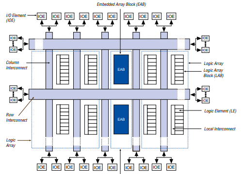
Architectural Overview
Figure 1 illustrates the FLEX 10K architecture:
- Groups of LEs are organized into LABs.
- LABs are arranged in rows and columns, with each row containing an Embedded Array Block (EAB).
- LABs and EABs are interconnected through the FastTrack Interconnect.
- IOEs are positioned at the ends of the rows and columns of the interconnect, linking the device core to external pins.
Logic Array
The FLEX 10K logic array is made up of Logic Array Blocks (LABs). Each LAB contains eight Logic Elements (LEs) and a local interconnect.
- Logic Elements (LEs): Each LE consists of a 4-input look-up table (LUT), a programmable flipflop, and dedicated signal paths for carry and cascade operations.
- LAB Functionality: The eight LEs in a LAB can implement medium-sized logic blocks such as 8-bit counters, address decoders, or state machines. Multiple LABs can be combined to form larger, more complex logic structures. Each LAB corresponds to roughly 96 usable gates.
FastTrack Interconnect
Signal routing within FLEX 10K devices and between device pins is handled by the FastTrack Interconnect, a network of fast, continuous row and column channels spanning the entire device.
I/O Elements (IOEs)
Each I/O pin connects to an I/O Element (IOE) at the ends of the FastTrack Interconnect rows and columns.
- Each IOE contains a bidirectional I/O buffer and an optional flipflop, which can serve as an input, output, or bidirectional register.
- With a dedicated clock pin, these registers offer excellent performance: – Inputs: setup times as low as 1.6 ns, hold times of 0 ns – Outputs: clock-to-output times as low as 5.3 ns
- IOEs also support JTAG BST, slew-rate control, tri-state buffers, and open-drain outputs.
Architectural Overview
Figure 1 illustrates the FLEX 10K architecture:
- Groups of LEs form LABs.
- LABs are arranged in rows and columns, with each row containing an Embedded Array Block (EAB).
- LABs and EABs are interconnected via the FastTrack Interconnect.
- IOEs are positioned at the ends of each row and column, linking the internal logic to the external pins.
FLEX 10K Device Block Diagram
FLEX 10K Device Block Diagram
Dedicated Control Inputs
FLEX 10K devices feature six dedicated inputs that directly drive the flipflops’ control signals, enabling high-speed, low-skew (under 1.5 ns) distribution of control signals. These signals are routed through dedicated channels, which provide shorter delays and lower skew than the standard FastTrack Interconnect.
Four of these dedicated inputs drive global signals, which can also be generated internally. This allows designers to implement features such as clock dividers or internally generated asynchronous clear signals that reset multiple registers across the device efficiently.
Embedded Array Block (EAB)
The Embedded Array Block (EAB) is a versatile RAM block with input and output registers, designed to implement common gate array megafunctions. Its flexibility and size make it well-suited for tasks such as multipliers, vector-scalar operations, and error-correction circuits.
EABs can be combined to support complex applications, including digital filters and microcontrollers, providing both high performance and functional versatility within a single FLEX 10K device.
Logic Implementation with Embedded Array Blocks (EABs)
In FLEX 10K devices, logic functions can be implemented by programming an EAB with a read-only pattern during configuration, effectively creating a large look-up table (LUT). Combinatorial functions are then executed by looking up results in the LUT rather than computing them dynamically. This approach often delivers faster performance than implementing the same function with general logic, a speed advantage amplified by the EAB’s rapid access times.
The large capacity of EABs allows complex functions to be implemented in a single logic level, avoiding the routing delays associated with multiple linked LEs or FPGA RAM blocks. For instance, a single EAB can implement a 4 × 4 multiplier with eight inputs and eight outputs. Parameterized functions, such as LPM functions, can automatically leverage the EAB for efficient implementation.
Advantages over FPGAs
Unlike FPGAs, which implement RAM as arrays of small, distributed blocks, EABs provide large, dedicated memory blocks with predictable timing and minimal routing issues. FPGA RAM blocks require interconnection to form larger memory structures, which introduces variable delays and routing challenges. In contrast, EABs eliminate these timing and routing concerns by providing a single, large memory block.
Synchronous RAM with EABs
EABs also simplify the implementation of synchronous RAM. With asynchronous RAM, the designer must generate the write enable (WE) signal and ensure that data and address signals meet setup and hold time requirements relative to WE. EABs, however, generate their own WE signals and are self-timed with respect to the global clock. Designers only need to meet the global clock’s setup and hold time requirements, making EAB-based RAM easier to use and more reliable than asynchronous alternatives.
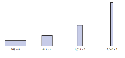
EAB Memory Configurations
Conclusion
FLEX 10K devices combine high-density logic arrays and flexible Embedded Array Blocks (EABs) to deliver fast, predictable, and efficient system-level performance. Their programmable architecture, large-capacity LUTs, and self-timed synchronous RAM simplify complex logic and memory implementations while reducing routing delays, offering designers a versatile and reliable platform for a wide range of applications.
Related Articles
Capacitance Basics: Grasp the Concept and Use the Formula
Motor Load, Wiring and Breaker Specifications for Efficient Operation
Band Reject Filters: Principles and Uses

Christopher Anderson
Christopher Anderson has a Ph.D. in electrical engineering, focusing on power electronics. He’s been a Senior member of the IEEE Power Electronics Society since 2021. Right now, he works with the KPR Institute of Engineering and Technology in the U.S. He also writes detailed, top-notch articles about power electronics for business-to-business electronics platforms.
Subscribe to JMBom Electronics !


