


QLSLAC™ Quad Audio-Processing ICs for Telecom Line Cards
Catalog
VE580 Series OverviewApplicationsKey FeaturesOrdering InformationProduct DescriptionQLSLAC Device ConfigurationsBlock DescriptionsPin DescriptionsKey Transmission SpecificationsConclusionRelated ArticlesVE580 Series Overview
The LE58QL02/021/031 Quad Low-Voltage Subscriber Line Audio-Processing Circuit (QLSLAC™) combines essential analog line card functions into a high-performance, highly programmable, four-channel codec-filter device. These QLSLAC devices build on the trusted design of Legerity’s proven SLAC™ family.
Featuring four independent channels, the QLSLAC devices use digital filters for software-controlled transmission, offering an efficient and cost-effective solution for the audio-processing needs of programmable line cards. They are fully compatible in software and coefficients with QSLAC devices.
Built with advanced submicron CMOS technology, the LE58QL02/021/031 QLSLAC devices deliver both low power consumption and rich functionality, making them ideal for maximizing line card density while minimizing costs. When paired with four Legerity SLIC devices, a single QLSLAC provides a complete, software-configurable solution for BORSCHT functions.
Applications
- Codec functionality for telephone switch line cards
Key Features
- Low-power 3.3 V CMOS technology with 5 V-tolerant digital inputs
- Fully software and coefficient compatible with LE79Q02/021/031 QSLAC™ devices
- Supports four codec/filter channels
- Software-programmable options include: SLIC device input impedance Transhybrid balance Transmit and receive gains Frequency-response equalization Digital I/O configuration Programmable input debouncing Time slot assignment Configurable clock slot and PCM transmit clock edge
- Standard microprocessor interface
- Supports A-law, µ-law, or linear coding
- Single or dual PCM ports available: Up to 128 channels per PCM port (PCLK at 8.192 MHz) Optional supervision on the PCM highway
- Master clock options: 1.536, 1.544, 2.048, 3.072, 3.088, 4.096, 6.144, 6.176, or 8.192 MHz, derived from MCLK or PCLK
- Built-in test modes including loopback, tone generation, and µP access to PCM data
- Mixed-state (analog and digital) impedance scaling
- Guaranteed performance over a 12 dB gain range
- Real-time data register with interrupt (open-drain or TTL output)
- Supports multiplexed SLIC device outputs and broadcast state
- 256 kHz or 293 kHz chopper clock for Legerity SLIC devices with switching regulator
- Maximum channel bandwidth suitable for V.90 modems
Related Documents
- 080754 – LE58QL061/063 QLSLAC™ Device Data Sheet
- 080761 – QSLAC™ to QLSLAC™ Device Design Conversion Guide
- 080758 – QSLAC™ to QLSLAC™ New Design Guide
Ordering Information
- All green packages comply with the RoHS Directive 2002/95/EC, reducing the environmental impact of electronic equipment.
- For tape-and-reel delivery, add a “T” suffix to the Ordering Part Number (OPN) when placing your order.
| Device | Package (Green)¹ | Packing² |
|---|---|---|
| LE58QL02FJC | 44-pin PLCC | Tube |
| LE58QL021FJC | 44-pin PLCC | Tube |
| LE58QL021BVC | 44-pin TQFP | Tray |
| LE58QL031DJC | 32-pin PLCC | Tube |
Product Description
The QLSLAC device integrates codec/filter and two-to-four-wire conversion functions needed for subscriber line interface circuitry in telecommunications equipment. It converts audio signals to digital PCM samples and vice versa, using digital filters to band-limit voice signals. All filtering is handled in digital signal processors driven by a master clock, derived from either PCLK or MCLK.
With four independent channels, the QLSLAC functions as four separate SLAC™ devices. Each channel has its own enable bit (EC1–EC4) for individual programming. Enabling multiple or all channels allows the same programming information to be broadcast, making initialization in large systems straightforward. Channel Enable bits are stored in the EC register, accessed via Command 4A/4Bh.
User-programmable digital filters allow control over receive and transmit gain, transhybrid balancing, two-wire termination impedance, and path equalization. Filter coefficients can be calculated using WinSLAC™ software.
PCM data can be transmitted or received as 8-bit companded codes (with optional 8-bit signaling in the transmit direction) or 16-bit linear codes. Compressed codes support A-law or µ-law formats. Data is read and written in user-defined PCM time slots, with rates from 128 kHz to 8.192 MHz. The transmit clock edge and clock slot are programmable for compatibility with other devices on the PCM highway.
Three QLSLAC configurations are available: single or dual PCM highways. LE58QL02 and LE58QL021 devices support dual and single PCM highways, respectively, in 44-pin packages. LE58QL031JC offers a single PCM highway in a 32-pin PLCC package.
QLSLAC Device Configurations
| PCM Highway | Programmable I/O per Channel | Chopper Clock | Package | Part Number |
|---|---|---|---|---|
| Dual | 4 I/O | Yes | 44-pin PLCC | LE58QL02JC |
| Single | 5 I/O | No | 44-pin PLCC/TQFP | LE58QL021JC (or VC) |
| Single | 2 I/O | No | 32-pin PLCC | LE58QL031JC |
Block Descriptions
Clock and Reference Circuits
Generates the master clock and frame sync signal for digital circuits, and provides an analog reference voltage for the analog circuits.
Microprocessor Interface (MPI)
Handles communication with an external control microprocessor via a serial interface. It transfers user control commands to other blocks and returns status information to the user. This block also contains the reset circuitry.
Time Slot Assigner (TSA)
Manages communication with the PCM highway, a time-division multiplexed bus carrying digitized voice samples. It implements programmable time slots and clocking arrangements for initial switching, and internally communicates with the Signal Processing Channels (CHx).
Signal Processing Channels (CHx)
Processes voice channel transmissions. The analog portion interfaces with VIN and VOUT pins, while the digital portion interfaces with the TSA block.
SLIC Device Interface (SLI)
Communicates digitally with SLIC device circuits, sending control bits to manage device modes, LEDs, and optocouplers. It also receives supervision information from SLIC devices and performs some signal filtering.
CONNECTION DIAGRAMS
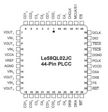
Le58QL02JC 44-Pin PLCC
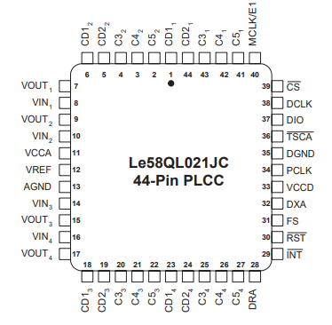
Le58QL021JC 44-Pin PLCC
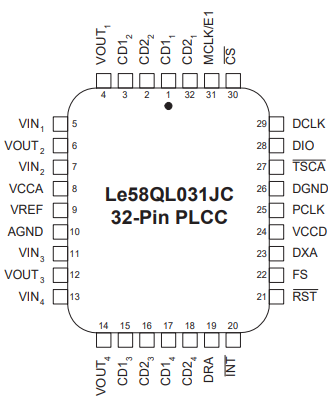
Le58QL031JC 32-Pin PLCC
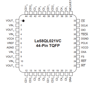
Le58QL021VC 44-Pin PLCC
Pin Descriptions
AGND, DGND – Power
Separate analog and digital grounds are provided to isolate noise. Internally, these grounds are connected, and they must also be connected on the circuit board.
CD11–CD14, CD21–CD24 – Inputs/Outputs (Control and Data)
CD1 and CD2 are TTL-compatible programmable I/O ports used to monitor or control the SLIC device or other subscriber line interface devices. Direction (input/output) is set via MPI Command 54/55h.
- As outputs, CD1/CD2 can control relays, LEDs, or other devices needing latched TTL signals (MPI Command 52h).
- As inputs, they can be processed by the QLSLAC device. CD1 supports programmable debounce (0–15 ms in 1 ms steps, MPI Command C8/C9h). CD2 supports filtering via the up/down counter and programmable sampling interval (MPI Command E8/E9h).
CD1 can also be demultiplexed for use with SLIC devices supporting the ground key function, producing Off-Hook/Ring Trip and Ground Key signals. Processed CD1/CD2 information can be read per channel (MPI Command 53h) or for all four channels simultaneously (MPI Command 4D/4Fh), reducing processor overhead for time-critical signals.
C31–C34, C41–C44, C51–C54 – Inputs/Outputs (Control)
C3, C4, and C5 are TTL-compatible programmable I/Os for monitoring or controlling SLIC or related devices. Direction is set via MPI Command 54/55h. Outputs control relays, LEDs, or other devices (MPI Command 52h). Inputs are accessed via MPI Command 53h.
- LE58QL021: Single PCM highway, five programmable I/Os per channel (CD1, CD2, C3, C4, C5), 44-pin PLCC/TQFP.
- LE58QL02: Dual PCM highways, four programmable I/Os per channel (C51–C54 removed), 44-pin PLCC/TQFP, supports chopper clock output.
- LE58QL031: Single PCM highway, two I/Os per channel (CD1, CD2), 32-pin PLCC.
CHCLK – Output (Chopper Clock)
Provides a 256 kHz or 292.57 kHz TTL-compatible clock for up to four SLIC devices with switching regulators. Synchronous to the master clock; phase is random. Not available in all packages.
CS – Input (Chip Select)
Active-low input enabling the device for control data write/read. Channels for operations are selected via the Channel Enable Register (EC1–EC4, Command 4A/4Bh). Holding CS low for 16 DCLK rising edges triggers a hardware reset when released.
DCLK – Input (Data Clock)
Shifts data into/out of the microprocessor interface. Maximum clock rate: 8.192 MHz.
DIO – Input/Output (Data)
Serial interface for control data, MSB first. Data rate is determined by DCLK. DIO is high-impedance when not transmitting.
DRA, DRB – Inputs (PCM Data Receive A/B)
Serially receives PCM data for channels 1–4 on either DRA or DRB during user-programmed time slots. Data is MSB first.
- Compressed signals: 1 byte per channel every 125 µs at PCLK rate.
- Linear signals: 2 bytes per channel every 125 µs.
- DRB is not available in all package types.
DXA, DXB – Outputs (PCM Data Transmit)
Transmits channel data serially via DXA or DXB during programmed time slots, MSB first.
- Output bursts: 8-bit (16-bit for Linear or PCM Signaling) every 125 µs.
- High-impedance between time slots or when inactive.
- DXB not available in all package types.
FS – Input (Frame Sync)
8 kHz pulse identifying Time Slot 0/Clock Slot 0. References all time slots relative to this signal; must be synchronized to PCLK.
INT – Output (Interrupt)
Active-low output, programmable as TTL or open-drain.
- Goes low when a Real-Time Data register bit changes or new transmit data appears (if armed).
- Remains low until the register is read or after a software/hardware reset.
- Individual CDxy bits can be masked (MPI Command 6C/6Dh). Transmit data interrupt is armed via the Operating Conditions register.
MCLK/E1 – Input/Output
- Master Clock input: 1.536, 1.544, or 2.048 MHz (×1, 2, or 4) for the DSP.
- Can function as E1 output to control Legerity SLIC devices with multiplexed hookswitch and ground-key outputs.
PCLK – Input (PCM Clock)
Controls the serial shift rate of PCM data. Must be an integer multiple of FS.
- Max: 8.192 MHz; Min: 128 kHz (dual PCM), 256 kHz (single PCM).
- Min clock doubles for Linear or PCM Signaling states.
- Frequencies between 1.03–1.53 MHz are not allowed.
- DSP clock can optionally be derived from PCLK.
RST – Input (Reset)
Logic-low resets the device to default state. May be tied to VCCD if unused.
TSCA, TSCB – Outputs (Time Slot Control)
Open-drain, normally inactive (Hi-Z). Active-low when transmitting PCM data on DXA or DXB, respectively. Pull-up resistors to VCCD required.
VCCA, VCCD – Power
Analog and digital supply inputs, separated for noise isolation. All VCC pins should be tied together at the PCB connector for optimal performance.
VIN1–VIN4 – Inputs (Analog)
Analog voice-band input for channels 1–4. Biased at VREF via internal resistor. Signals are sampled, processed, and output as TTL PCM data. Saturation pulls VIN toward AGND (negative) or VCCD (positive).
VOUT1–VOUT4 – Outputs (Analog)
Analog output for processed PCM data of channels 1–4. Referenced to VREF.
VREF – Output (Analog Voltage Reference)
Provides a reference voltage; connect an external capacitor to ground to filter noise. Buffered for internal circuitry. Ensure low leakage current.
Absolute Maximum Ratings
Exceeding the limits listed below may cause permanent damage to the device. Proper operation at or beyond these values is not guaranteed. Prolonged exposure may reduce device reliability.
Package Assembly
Green package devices are assembled using environmentally compatible, Pb-free, halogen-free, and antimony-free materials. Leads feature matte-tin plating compatible with conventional or lead-free PCB assembly processes.
- Refer to IPC/JEDEC J-Std-020: Table 4-2 for peak soldering temperatures and Table 5-2 for recommended solder reflow profiles.
Operating Ranges
Performance is guaranteed across:
- Commercial: 0 °C to 70 °C
- Industrial: -40 °C to 85 °C
Electrical characterization and production tests are conducted per Bellcore GR-357-CORE Section 4.6.2 to ensure reliability.
Environmental Limits
- Storage Temperature: -60 °C to +125 °C
- Ambient Temperature (under bias): -40 °C to +85 °C
- Relative Humidity (non-condensing): 5–95%
Electrical Limits
- VCCA vs AGND: -0.4 V to +4.0 V
- VCCA vs VCCD: ±0.4 V
- VCCD vs DGND: -0.4 V to +4.0 V
- VIN vs AGND: -0.4 V to (VCCA + 0.4 V)
- AGND vs DGND: ±50 mV
- Digital pins vs DGND: -0.4 V to 5.5 V or VCCD + 2.37 V, whichever is lower
Current Ratings
- Total CD1–C5 per device: 40 mA source from VCCD, 40 mA sink into DGND
- Latch-up immunity (any pin): ±100 mA
- Total VCC current (rise rate > 0.4 V/µs): 0.5 A
Environmental Ranges
- Ambient Temperature: -40 °C to +85 °C
- Ambient Relative Humidity: 15 % to 85 %
Electrical Ranges
- Analog Supply (VCCA): 3.3 V ±5 %
- Digital Supply (VCCD): VCCD ±50 mV
- DGND: 0 V
- AGND: ±10 mV
- CFL1 Capacitance (VREF to AGND): 0.1 µF ±20 %
- Digital Pins: DGND to +5.25 V
Electrical Characteristics
Typical values are at TA = 25 °C and nominal supply voltages. Min/Max values cover the full temperature and supply ranges shown under Operating Ranges unless otherwise noted.
| Symbol | Parameter | Min | Typ | Max | Unit | Notes |
|---|---|---|---|---|---|---|
| VIL | Digital Input Low Voltage | – | – | 0.8 | V | – |
| VIH | Digital Input High Voltage | 2.0 | – | – | V | – |
| IIL | Digital Input Leakage Current | –7 | – | +7 | µA | 0 < V < VCCD; otherwise –120 to +180 |
| VHYS | Digital Input Hysteresis | 0.16 | 0.25 | 0.34 | V | – |
| VOL | Digital Output Low Voltage | 0.4 | – | 0.8 | V | CD1–C5 (IOL = 4/8 mA), TSCA/TSCB (IOL = 14 mA), other outputs (IOL = 2 mA) |
| VOH | Digital Output High Voltage | 2.4 | – | VCCD – 0.4/0.8 | V | CD1–C5 (IOH = 4/8 mA), other outputs IOH = 400 µA |
| IOL | Digital Output Leakage Current (Hi-Z) | –7 | – | +7 | µA | 0 < V < VCCD; otherwise –120 to +180 |
| GIN | Input Attenuator Gain | 0.6438 | 1 | – | V/V | DGIN = 0 or 1 |
| VIR | Analog Input Voltage Range (vs VREF) | ±0.792 | ±1.02 | ±1.584 | Vpk | Depends on attenuator setting |
| VIOS | VIN Offset Voltage | –50 | – | 50 | mV | – |
| ZIN | Analog Input Impedance (300–3400 Hz) | 600 | – | 1400 | kΩ | – |
| IIP | Input Current (VIN = 3.3 V) | – | 50 | 115 | µA | – |
| IIN | Input Current (VIN = –0.3 V) | – | 50 | 130 | µA | – |
| ZOUT | VOUT Output Impedance | 1 | – | 10 | Ω | – |
| CLOUT | Allowable Capacitance (VOUT to AGND) | – | – | 500 | pF | – |
| IOUT | VOUT Output Current (f < 3400 Hz) | –4 | – | 4 | mApk | – |
| VREF | VREF Output Voltage (open circuit, leakage < 20 nA) | 1.43 | 1.5 | 1.57 | V | – |
| ZREF | VREF Output Impedance (f < 3400 Hz) | 70 | – | 130 | kΩ | – |
| VOR | VOUT Voltage Range (vs VREF) | ±0.51 | – | ±1.02 | Vpk | AR = 0 or 6.02 dB |
| VOOS | VOUT Offset Voltage (AISN off) | –40 | – | 40 | mV | – |
| VOOSA | VOUT Offset Voltage (AISN on) | –80 | – | 80 | mV | – |
| GAISN | AISN Gain (Input = 0 dBm0, 1014 Hz) | –0.024 | – | 0.024 | V/V | DGIN = 0/1 |
| PD | Power Dissipation | 13 | 40–130 | 170 | mW | All channels active, 1 channel active, all inactive |
| CI | Digital Input Capacitance | – | 10 | – | pF | – |
| CO | Digital Output Capacitance | – | 10 | – | pF | – |
| PSRR | Power Supply Rejection Ratio (1.02 kHz, 100 mVRMS) | 40 | – | – | dB | GX = GR = 0 dB |
Notes
- The CD1, CD2, and C3–C5 outputs are resistive for voltage drops below 0.8 V. Total current must remain within the absolute maximum ratings.
- If the digitizer saturates, a 50 kΩ ±20 kΩ resistor connects to either AGND or VCCA to discharge the coupling capacitor.
- In the Inactive state, VOUT presents either a VREF DC level through a 15 kΩ resistor (VMODE = 0) or high impedance (VMODE = 1).
- With an external DC path from VOUT to VIN of gain GDC, and AISN gain hAISN, the output offset is multiplied by 1 / [1 – (hAISN • GDC)].
- In the Inactive state, power dissipation is measured with all digital inputs at VIH = VCCD or VIL = DGND and no load on VOUT1–VOUT4.
Transmission Characteristics
Unless otherwise noted, relative signal levels are in dBm0. Specifications apply for GX = 0–12 dB, GR = 0–12 dB, and input attenuator (GIN) on or off.
Notes
- See Figure 5 and Figure 6 for measurement setups.
- Input: 0 dBm0, 300–3400 Hz; measurements at other frequencies use the same range.
- No single frequency above 3800 Hz may exceed –55 dBm0.
- Crosstalk weighted average is calculated as:Weighted Crosstalk=∑jC(fj),f1=300 Hz, fN=3300 Hz, j=2..N\text{Weighted Crosstalk} = \sum_j C(f_j), \quad f_1 = 300\,\text{Hz}, \, f_N = 3300\,\text{Hz}, \, j = 2..NWeighted Crosstalk=j∑C(fj),f1=300Hz,fN=3300Hz,j=2..N
0 dBm0 Voltage Definitions (Unity Gain: X, R, GX, GR, AX, AR)
| Signal | DGIN = 0 | DGIN = 1 | Receive | Unit |
|---|---|---|---|---|
| A-law digital | 0.7804 | 0.5024 | 0.5024 | mW |
| µ-law digital | 0.7746 | 0.4987 | 0.4987 | mW |
| Linear-coded sine ±22,827 peak | 0.7804 | 0.5024 | 0.5024 | Vrms |
Key Transmission Specifications
| Parameter | Test Conditions | Min | Typ | Max | Unit | Notes |
|---|---|---|---|---|---|---|
| Gain Accuracy, D/A or A/D | 0 dBm0, 1014 Hz, AX=AR=0 dB | –0.25 | – | 0.25 | dB | 0–85 °C |
| Gain Accuracy, AX=+6.02 dB or AR=–6.02 dB | –0.30 | – | 0.30 | dB | –40–85 °C | |
| Digital-to-Digital Gain Accuracy | –0.25 | – | 0.25 | dB | – | |
| Analog-to-Analog Gain Accuracy | –0.25 | – | 0.25 | dB | – | |
| Attenuation Distortion | 300–3000 Hz | –0.125 | – | 0.125 | – | 1 |
| Single-Frequency Distortion | – | –46 | – | – | dBm0 | 2 |
| Second Harmonic Distortion, D/A, GR=0 dB | – | –55 | – | – | dBm0 | – |
| Idle Channel Noise | Analog Out | 0 | – | – | dBm0p | 3 |
| Idle Channel Noise | Digital Out | 0 | – | – | dBm0 | 3 |
| Idle Channel Noise | Digital Loopback Weighted | – | –68 | – | dBrnc0 | 3,6 |
| Idle Channel Noise | Digital Loopback Unweighted | – | –55 | – | dBm0p | 3,6 |
| Crosstalk TX→RX same channel | 0 dBm0, 300–3400 Hz | –75 | – | – | dBm0 | – |
| Crosstalk RX→TX same channel | 0 dBm0, 300–3400 Hz | –75 | – | – | dBm0 | – |
| Crosstalk Between Channels TX/RX | 0 dBm0, SLIC < 300 Ω, 1014 Hz Avg | –76 | – | – | dBm0 | 4 |
| Crosstalk Between Channels TX/RX | 0 dBm0, 1014 Hz Avg | –78 | – | – | dBm0 | 4 |
| End-to-End Group Delay | B=Z=0; X=R=1 | – | 678 | – | µs | 5 |
Conclusion
The Le58QL02/021/031 QLSLAC™ devices offer a highly integrated, low-voltage solution for subscriber line audio processing, combining four independent codec/filter channels with programmable two-to-four-wire conversion. Designed using advanced submicron CMOS technology, these devices deliver low power consumption, flexible software-controlled signal processing, and compatibility with Legerity SLIC devices for a complete, configurable BORSCHT solution. With support for single or dual PCM highways, precise analog and digital interfacing, and robust environmental and electrical performance, the QLSLAC devices provide an efficient, reliable, and cost-effective solution for modern telecommunications line card designs.
Related Articles
Capacitance Basics: Grasp the Concept and Use the Formula
Motor Load, Wiring and Breaker Specifications for Efficient Operation
Band Reject Filters: Principles and Uses

Amanda Miller
Amanda Miller is a senior electronics engineer with 6 years of experience. She focuses on studying resistors, transistors, and package design in detail. Her deep knowledge helps her bring innovation and high standards to the electronics industry.
Subscribe to JMBom Electronics !


