
Texas Instruments INA226AIDGSR


- Part Number:
INA226AIDGSR
- Manufacturer:
- Category:
- RoHs:
 RoHS Compliant
 - Datasheet:
 INA226AIDGSR_Datesheet
 - Description:
Current Monitor Regulator High/Low-Side 10mA 10-VSSOP
- In stock 15,266

INA226AIDGSR Datasheet Comprehensive Summary
1. Overview
The INA226AIDGSR is a high-precision, 16-bit current, voltage, and power monitor from Texas Instruments (TI), designed for high-side or low-side sensing in power management systems. It features an I2C/SMBus-compatible interface, supports bus voltages up to 36V, and operates from a 2.7V to 5.5V supply. Packaged in a compact 10-pin VSSOP (DGS) format, this device delivers ultra-accurate measurements (0.1% maximum gain error, 10μV maximum offset) and flexible configuration via programmable registers—ideal for rack servers, wireless infrastructure, high-performance computing, and battery monitoring applications.
2. Key Features
2.1 Core Measurement Capabilities
- Wide Voltage Range: Monitors bus voltages (VBUS) from 0V to 36V and shunt voltages (VSENSE) from -81.9175mV to +81.92mV.
- High Accuracy:
- Derived Metrics: Calculates current (via external shunt resistor) and power (25× current LSB) using an internal multiplier, with direct digital readouts.
2.2 Configuration & Control
- Programmable Averaging: 8 options (1, 4, 16, 64, 128, 256, 512, 1024 samples) to filter noise and improve accuracy.
- Adjustable Conversion Times: 8 settings for shunt/bus voltage ADC (140μs to 8.244ms) to balance speed and precision.
- 16 I2C Addresses: Configurable via A0/A1 pins (connect to GND, VS, SDA, or SCL) for multi-device bus operation.
- Alert Functionality: Open-drain Alert pin for 5 user-defined events (shunt over/under-limit, bus over/under-limit, power over-limit) plus conversion-ready notification.
2.3 Environmental & Mechanical Specifications
- Temperature Range: -40°C to +125°C (operating); -65°C to +150°C (storage).
- Power Efficiency: Typical quiescent current (IQ) of 330μA (active mode), 0.5μA (power-down mode).
- ESD Protection: ±2500V (Human Body Model), ±1000V (Charged Device Model).
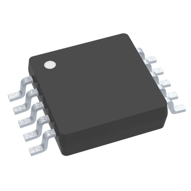
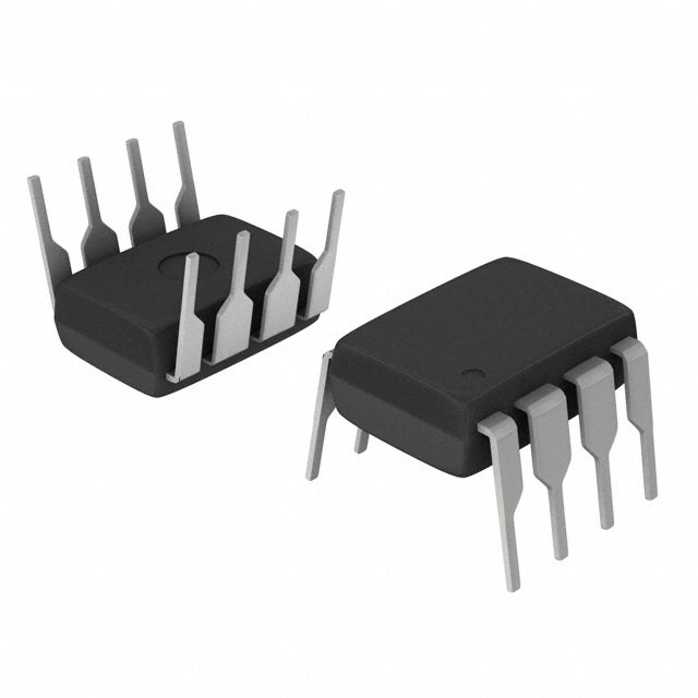
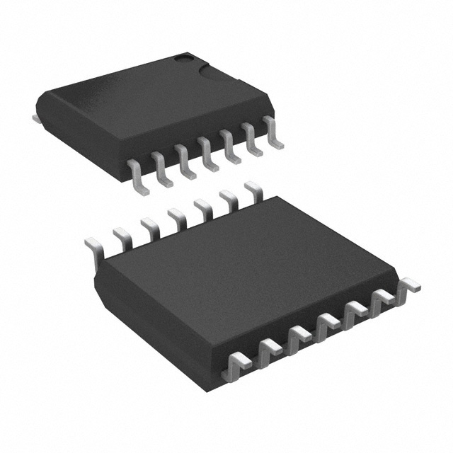
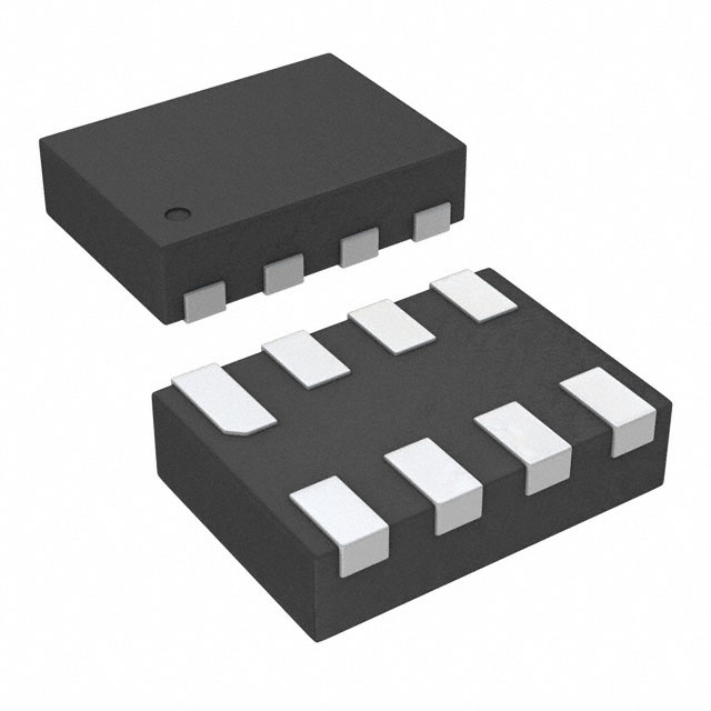
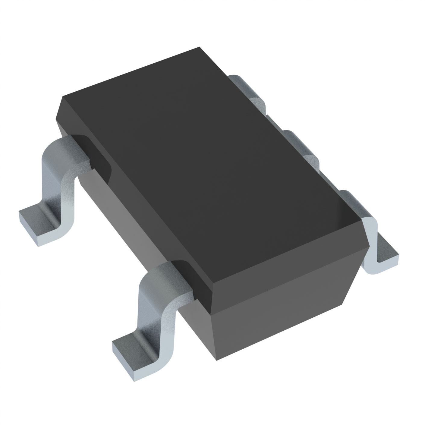
- Package: 10-pin VSSOP (DGS); dimensions: 3.00mm × 4.90mm × 1.1mm (max height).
3. Pin Configuration & Function
The INA226AIDGSR uses a 10-pin VSSOP package (top-view orientation) with dedicated pins for analog inputs, power, digital communication, and control. Key pin details are summarized below:
| Pin # | Pin Name | I/O Type | Core Function | Key Notes |
|---|---|---|---|---|
| 1 | A1 | Digital Input | I2C address pin 1 | Connect to GND/VS/SDA/SCL (see Table 6-2 for address mapping) |
| 2 | A0 | Digital Input | I2C address pin 0 | Works with A1 to set 1 of 16 slave addresses |
| 3 | Alert | Digital Output | Multi-functional alert (open-drain) | Triggers on user-defined limits or conversion ready; pull-up required |
| 4 | SDA | Digital I/O | I2C/SMBus data line | Open-drain; requires external pull-up resistor |
| 5 | SCL | Digital Input | I2C/SMBus clock line | Open-drain; requires external pull-up resistor |
| 6 | VS | Analog Input | Power supply (2.7V to 5.5V) | Bypass to GND with 0.1μF ceramic capacitor |
| 7 | GND | Analog | Ground | Connect to battery/load negative terminal; use low-impedance path |
| 8 | VBUS | Analog Input | Bus voltage input | Monitors power supply bus (0V to 36V); connect to system VBUS |
| 9 | IN– | Analog Input | Shunt resistor load side | Connect to load-side of external shunt resistor |
| 10 | IN+ | Analog Input | Shunt resistor supply side | Connect to supply-side of external shunt resistor |
4. Electrical Specifications (TA = -40°C to +125°C, VS = 3.3V, VIN+ = 12V, VSENSE = 0mV, VBUS = 12V)
4.1 Critical Measurement Parameters
| Parameter | Test Conditions | Min | Typ | Max | Unit |
|---|---|---|---|---|---|
| Shunt Voltage Range | -- | -81.9175 | -- | 81.92 | mV |
| Bus Voltage Range | -- | 0 | -- | 36 | V |
| Shunt Voltage Gain Error | -- | -- | -- | 0.1 | % |
| Bus Voltage Gain Error | -- | -- | -- | 0.1 | % |
| Shunt Offset Voltage (RTI) | -- | -2.5 | -- | +10 | μV |
| Bus Offset Voltage (RTI) | -- | -1.25 | -- | +7.5 | mV |
| Common-Mode Rejection Ratio (CMRR) | 0V ≤ VIN+ ≤ 36V | 126 | 140 | -- | dB |
4.2 ADC & Timing Parameters
| Parameter | Test Conditions | Min | Typ | Max | Unit |
|---|---|---|---|---|---|
| ADC Conversion Time (tCT) | CT bits = 000 (fastest) | 140 | -- | 154 | μs |
| ADC Conversion Time (tCT) | CT bits = 111 (slowest) | 8.244 | -- | 9.068 | ms |
| SMBus Timeout | -- | 28 | -- | 35 | ms |
| Input Bias Current (IN+/IN–) | -- | -- | 0.1 | -- | nA |
4.3 Power & Digital Interface
| Parameter | Test Conditions | Min | Typ | Max | Unit |
|---|---|---|---|---|---|
| Supply Voltage (VS) | -- | 2.7 | 3.3 | 5.5 | V |
| Quiescent Current (IQ) | Active mode | -- | 330 | 420 | μA |
| Quiescent Current (IQ) | Power-down mode | -- | 0.5 | 2 | μA |
| I2C Bus Frequency | Fast mode | 0.001 | -- | 0.4 | MHz |
| I2C Bus Frequency | High-speed mode | 0.001 | -- | 2.94 | MHz |
| High-Level Input Voltage (VIH) | -- | 0.7×VS | -- | 6 | V |
| Low-Level Input Voltage (VIL) | -- | -0.5 | -- | 0.3×VS | V |
5. Register Set & Programming
The INA226AIDGSR uses 10 registers (8 main registers + 2 ID registers) for configuration, measurement storage, and alert control. All registers are 16-bit and accessed via I2C (MSB first). Key registers are summarized below:
| Register Address | Register Name | Type | Core Function | Power-On Reset Value |
|---|---|---|---|---|
| 00h | Configuration | R/W | Sets conversion time, averaging, operating mode (continuous/triggered/power-down); system reset | 4127h (0100000100100111b) |
| 01h | Shunt Voltage | R | Stores 16-bit shunt voltage measurement (2.5μV LSB) | 0000h |
| 02h | Bus Voltage | R | Stores 16-bit bus voltage measurement (1.25mV LSB) | 0000h |
| 03h | Power | R | Calculated power (25× Current LSB); 0 until Calibration register is programmed | 0000h |
| 04h | Current | R | Calculated current (via shunt resistor); 0 until Calibration register is programmed | 0000h |
| 05h | Calibration | R/W | Sets current LSB and shunt resistor value; enables current/power calculations | 0000h |
| 06h | Mask/Enable | R/W | Configures Alert pin (function, polarity, latching); conversion ready flag (CVRF) | 0000h |
| 07h | Alert Limit | R/W | Threshold value for selected alert function (e.g., shunt over-limit) | 0000h |
| FEh | Manufacturer ID | R | TI’s unique ID: 5449h (0101010001001001b) | 5449h |
| FFh | Die ID | R | Device ID + revision: 2260h (0010001001100000b) | 2260h |
5.1 Critical Programming Equations
- Current LSB Calculation: Determines current resolution based on maximum expected current:CurrentLSB=215Maximum Expected Current
- Calibration Register (CAL): Programs shunt resistor value (R_SHUNT) and Current_LSB for accurate current/power calculations:CAL=CurrentLSB×RSHUNT0.00512
- Current Calculation: Derived from shunt voltage and CAL register:Current=2048Shunt Voltage Register×CAL
- Power Calculation: Derived from current and bus voltage:Power=2000Current Register×Bus Voltage Register
6. Operating Modes
6.1 Measurement Modes
Controlled via the Configuration Register (00h, MODE bits [2:0]):
- Continuous Mode (default): Continuously measures shunt + bus voltage, averages samples, and updates registers. Options:
- Triggered Mode: Single-shot measurement (triggers on register write). Options:
- Power-Down Mode (000b/100b): Reduces IQ to 0.5μA (max); registers remain accessible.
6.2 Alert Functionality
Configured via the Mask/Enable Register (06h) and Alert Limit Register (07h):
- Alert Functions: 5 options (only 1 active at a time, highest bit priority):
- Alert Behavior:
7. Recommended External Components
| Component | Type | Value | Purpose |
|---|---|---|---|
| Shunt Resistor (R_SHUNT) | Precision current-sense | User-defined (e.g., 2mΩ for 10A max current) | Converts load current to measurable voltage (VSENSE = I_LOAD × R_SHUNT) |
| VS Bypass Capacitor | Ceramic (low-ESR) | 0.1μF | Filters supply noise; place close to VS (Pin 6) and GND (Pin 7) |
| I2C Pull-Up Resistors | Carbon-film | 1kΩ to 10kΩ | Required for SDA (Pin 4) and SCL (Pin 5); value depends on bus length/frequency |
| Input Filter (Optional) | Series resistor + capacitor | R ≤10Ω, C=0.1μF–1μF | Reduces high-frequency noise on IN+/IN–/VBUS pins |
8. Layout Guidelines
To ensure accuracy and minimize noise, follow these PCB layout best practices:
- Kelvin Connection: Use 4-wire sensing for the shunt resistor (IN+/IN– pins) to avoid including trace resistance in measurements.
- Grounding:
- Trace Routing:
- Component Placement:
9. Ordering Information & Package Details
| Part Number | Package Type | Pin Count | Temperature Range | Packaging | RoHS Compliance | MSL Rating |
|---|---|---|---|---|---|---|
| INA226AIDGSR | VSSOP (DGS) | 10 | -40°C to +125°C | Tape & Reel (2500 units) | Yes | Level 2 (260°C, 1 year) |
| INA226AIDGST | VSSOP (DGS) | 10 | -40°C to +125°C | Tape & Reel (250 units) | Yes | Level 2 (260°C, 1 year) |
9.1 Package Dimensions (VSSOP DGS)
- Length: 4.75mm–5.05mm
- Width: 2.9mm–3.1mm
- Height: 1.1mm (max)
- Lead Pitch: 0.5mm
10. Typical Applications
The INA226AIDGSR is ideal for high-reliability power monitoring systems, including:
- Rack servers and data center infrastructure
- Wireless base stations and telecom equipment
- High-performance computing (HPC) systems
- Battery cell monitors and balancers
- Industrial power supplies and test equipment
- Automotive infotainment (via automotive-qualified INA226-Q1 variant)
11. Key Safety & Reliability Notes
- Voltage Limits: Do not exceed 36V on VBUS or ±40V differential on IN+/IN– (common-mode voltage: -0.3V to 40V).
- ESD Handling: Follow JEDEC J-STD-020A for reflow soldering; avoid hand/wave soldering.
- Calibration: Program the Calibration Register (05h) before using current/power measurements (registers default to 0).
- Thermal Management: The VSSOP package has a junction-to-ambient thermal resistance (RθJA) of 144.6°C/W; avoid placing heat-generating components nearby.
Purchase
No need to register to order from JMBom Electronics, but signing in lets you track your order like a pro. Give it a try for a smoother shopping ride.
Means
Easy peasy! Pay your way with PayPal, Credit Card, or wire transfer in USD. We've got you covered.
RFQ(Request for Quotations)
Get the freshest prices and stock updates by asking for a quote! Our sales team will shoot you an email within a day. It's that simple.
IMPORTANT NOTICE
1. Look out for your order details in your inbox! (If it's missing, check the spam folder just in case.)
2. Our sales manager will double-check the order and keep you posted on any price or stock changes. No worries, we've got you covered.

Shipping Rate
We ship orders once a day around 5 p.m., except Sunday. Once shipped, the estimated delivery time depends on the courier company you choose, usually 5-7 working days.

Shipping Methods
We provide DHL, FedEx, UPS, EMS, SF Express, and Registered Air Mail international shipping.


Payment
You can pay the orders on the website directly or pay by wire transfer offline. We support: Paypal、VISA、Credit Card.


Texas Instruments
Texas Instruments
Texas Instruments
Texas Instruments
Texas Instruments
Texas Instruments
Texas Instruments
Texas Instruments
Texas Instruments
Texas Instruments
Texas Instruments

Texas Instruments