
Renesas SLG46538-AP


- Part Number:
SLG46538-AP
- Manufacturer:
- Category:
- RoHs:
 Non-RoHS Compliant
 - Datasheet:
- Description:
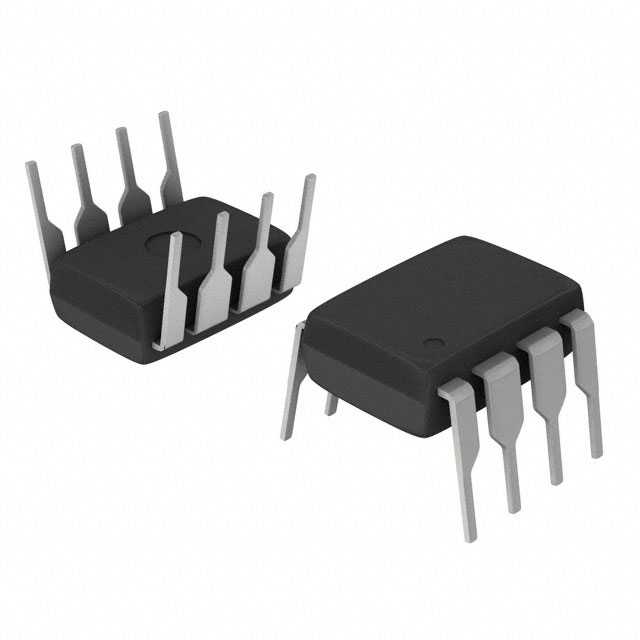
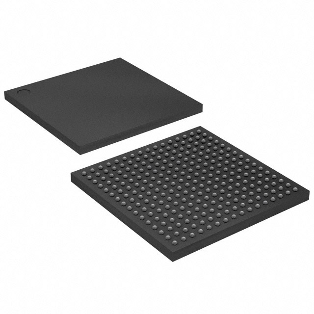
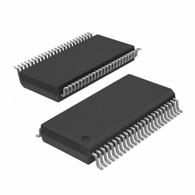
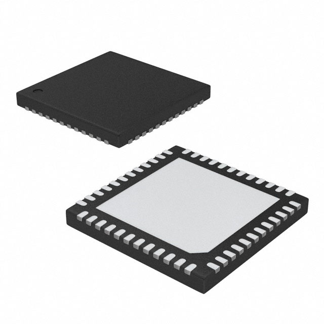
IC CPLD 19MC 20TQFN
- In stock 0

SLG46538-AP Datasheet Summary
1. Overview
The SLG46538 is a highly versatile programmable mixed-signal matrix from Renesas’ GreenPAK family, integrated with an asynchronous state machine and dual-supply capability. It enables users to implement diverse mixed-signal functions in a compact, low-power single IC by programming one-time Non-Volatile Memory (NVM) to configure interconnect logic, I/O pins, and macrocells. The dual-supply feature (VDD and VDD2) supports interfacing two independent voltage domains, facilitating level translation and cross-domain mixed-signal designs.
2. Key Features
2.1 Core Capabilities
- Dual-Supply Operation: VDD and VDD2 range from 1.8 V (±5%) to 5 V (±10%), with VDD2≤VDD
- Mixed-Signal Macrocells: 4 analog comparators (ACMP), 2 voltage references (Vref), 19 combination function macrocells (LUTs, DFFs, counters/delays, etc.)
- State Machine: 8 states with flexible input logic for state transitions
- Serial Communication: I2C protocol compliance
- Memory: 8-byte RAM (I2C-readable/writable) + OTP user memory
- Oscillators: Configurable 25 kHz/2 MHz RC oscillator, 25 MHz RC oscillator, and crystal oscillator
- Additional Functions: Programmable delay, edge detectors, deglitch filters, inverter, analog temperature sensor
2.2 Environmental & Compliance
- Operating Temperature Range: -40 °C to 85 °C
- Storage Temperature Range: -65 °C to 150 °C
- RoHS Compliant / Halogen-Free
- ESD Protection: 2000 V (Human Body Model), 500 V (Charged Device Model)
- Moisture Sensitivity Level: 1
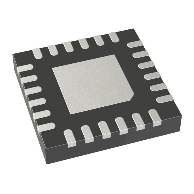
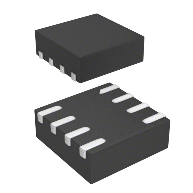
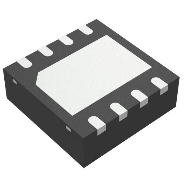
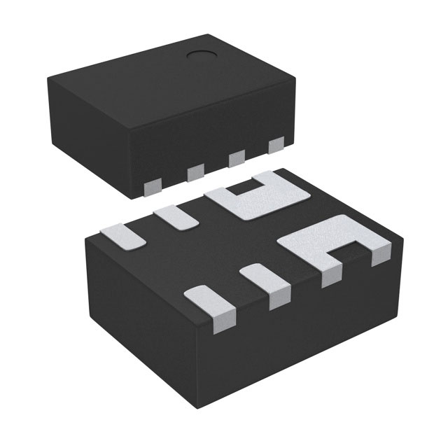
3. Package Options
| Package Type | Pin Count | Dimensions (mm) | Pitch (mm) | Part Number |
|---|---|---|---|---|
| STQFN | 20 | 2 x 3 x 0.55 | 0.4 | SLG46538V |
| MSTQFN | 22 | 2 x 2.2 x 0.55 | 0.4 | SLG46538M |
- Tape and Reel (3k units) is the default shipping format; "TR" suffix is legacy and no longer used.
4. Pin Description
4.1 Power Pins
- VDD: Primary power supply (Pin 1 for STQFN-20, Pin 16 for MSTQFN-22)
- VDD2: Secondary power supply (Pin 14 for STQFN-20, Pin 12 for MSTQFN-22)
- GND: Ground (Pin 11 for STQFN-20, Pin 20 for MSTQFN-22)
4.2 Key I/O Pins
- General Purpose I/O (IO0-IO17): Support digital/analog input/output, with options for Schmitt trigger, low-voltage input, push-pull/open-drain output
- Special Function Pins:
4.3 Pin Configuration Notes
- IO0 is input-only; all other IOs support bidirectional operation
- IOs 0-8 are powered by VDD; IOs 9-17 are powered by VDD2
- Pull-up/pull-down resistors (10 kΩ/100 kΩ/1 MΩ) are configurable for all IOs (IO0 has fixed pull-down)
5. Electrical Specifications
5.1 Absolute Maximum Ratings
| Parameter | Min. | Max. | Unit |
|---|---|---|---|
| Supply Voltage (VDD) | -0.5 | 7 | V |
| Supply Voltage (VDD2) | -0.5 | VDD+0.5 | V |
| DC Input Voltage | -0.5 | VDD+0.5 | V |
| Maximum Output Current | -- | 43 (OD 4X) | mA |
| Junction Temperature | -- | 150 | °C |
5.2 Typical Electrical Characteristics (3.3 V VDD)
| Parameter | Typ. | Unit |
|---|---|---|
| Quiescent Current (IQ) | 0.81 | µA |
| HIGH-Level Input Voltage (VIH) | 2.14 | V |
| LOW-Level Input Voltage (VIL) | 0.97 | V |
| HIGH-Level Output Voltage (VOH) | 3.12 | V |
| LOW-Level Output Voltage (VOL) | 0.06 | V |
| Schmitt Trigger Hysteresis (VHYS) | 0.62 | V |
5.3 I2C Specifications
- Clock Frequency (FSCL): Up to 400 kHz
- Clock Low Pulse Width (tLOW): 1300 ns min.
- Clock High Pulse Width (tHIGH): 600 ns min.
- Data Setup Time (tSU_DAT): 100 ns min.
6. User Programmability
6.1 Configuration Flow
- Design creation in GreenPAK Designer software
- Emulation (on-chip, no NVM programming) for rapid testing
- NVM programming with GreenPAK development tools for samples
- Production integration by forwarding design files to Renesas
6.2 Non-Volatile Memory (NVM)
- One-Time-Programmable (OTP) for permanent configuration
- Emulation mode retains configuration while powered, supporting re-writes
- User-defined initial values for RAM are transferred from OTP during startup
7. Macrocell Details
7.1 Combination Function Macrocells
| Type | Quantity | Key Functions |
|---|---|---|
| 2-bit LUT/DFF | 3 | Combinatorial logic or edge-triggered storage |
| 3-bit LUT/DFF (with Set/Reset) | 5 | Enhanced storage with control inputs |
| 3-bit LUT/Pipe Delay | 1 | 16-stage delay with 3 outputs |
| 2-bit LUT/PGEN | 1 | Programmable pattern generation (2-16 bits) |
| 8-bit Counter/Delay | 5 | Timing control, frequency detection |
| 16-bit Counter/Delay | 2 | Extended timing range, FSM support |
| Deglitch Filters | 2 | Edge detection with glitch suppression |
7.2 Analog Comparators (ACMP)
- Input Voltage Range: 0 to VDD (positive), 0 to 1.2 V (negative)
- Hysteresis Options: 0 mV/25 mV/50 mV/200 mV
- Gain Options: 1x/0.5x/0.33x/0.25x
- Wake & Sleep control for power saving
7.3 State Machine
- 8 configurable states with user-defined transitions
- 24 input signals for state transitions + 1 reset input
- 8 output signals (user-programmable per state)
- Asynchronous operation (no clock required)
7.4 Oscillators
| Oscillator Type | Frequency Range | Key Features |
|---|---|---|
| RC Oscillator 0 | 25 kHz/2 MHz | Configurable, low power |
| RC Oscillator 1 | 25 MHz | High-frequency, for precision timing |
| Crystal Oscillator | 32.768 kHz-40 MHz | External crystal/ceramic resonator support |
8. Memory
8.1 RAM
- 8-byte capacity, readable/writable via I2C
- Retains data during operation; initial values from OTP
8.2 OTP Memory
- Stores user configuration (macrocells, connection matrix)
- Transfers initial RAM values during power-up
- Read-back protection (Read Lock) available
9. Applications
- Personal Computers and Servers
- PC Peripherals
- Consumer Electronics
- Data Communications Equipment
- Handheld and Portable Electronics
10. Ordering Information
| Part Number | Package Type | Description |
|---|---|---|
| SLG46538V | STQFN-20 | 20-pin STQFN, Tape and Reel |
| SLG46538M | MSTQFN-22 | 22-pin MSTQFN, Tape and Reel |
11. Key Design Considerations
- VDD2 must not exceed VDD at any time
- ACMP power-up time should be accounted for in timing-sensitive designs
- I2C protection bits (reg<1832>, reg<1870>, reg<1871>) control read/write access to registers
- Crystal oscillator requires external components (capacitors/resistors) for stability
Purchase
No need to register to order from JMBom Electronics, but signing in lets you track your order like a pro. Give it a try for a smoother shopping ride.
Means
Easy peasy! Pay your way with PayPal, Credit Card, or wire transfer in USD. We've got you covered.
RFQ(Request for Quotations)
Get the freshest prices and stock updates by asking for a quote! Our sales team will shoot you an email within a day. It's that simple.
IMPORTANT NOTICE
1. Look out for your order details in your inbox! (If it's missing, check the spam folder just in case.)
2. Our sales manager will double-check the order and keep you posted on any price or stock changes. No worries, we've got you covered.

Shipping Rate
We ship orders once a day around 5 p.m., except Sunday. Once shipped, the estimated delivery time depends on the courier company you choose, usually 5-7 working days.

Shipping Methods
We provide DHL, FedEx, UPS, EMS, SF Express, and Registered Air Mail international shipping.


Payment
You can pay the orders on the website directly or pay by wire transfer offline. We support: Paypal、VISA、Credit Card.


Renesas
Renesas
Renesas
Renesas

Renesas

Renesas
Renesas

Renesas
Renesas
Renesas
Renesas
Renesas