


Inverting Summing Amplifier: Circuit Diagram,Operation and Formula
Catalog
What Is an Inverting Summing Amplifier?Role of the Op-Amp in a Summing AmplifierHow an Op-Amp Works in a Summing Amplifier: Voltage Follower vs Inverting ModeInverting Summing Amplifier: How It WorksInverting vs. Non-Inverting Summing AmplifiersOutput Equation of an Inverting Summing AmplifierInverting Summing Amplifier: Transfer Function Derivation & Practical ExamplesDeriving the Transfer Function of an Inverting Summing AmplifierAdvantages and Disadvantages of an Inverting Summing AmplifierApplications of Inverting Summing AmplifierSummaryFrequently Ask QuestionsRelated ArticlesOne of the key functions of an operational amplifier (op-amp) is to act as a summing amplifier, also known as an adder. When the op-amp has a high input impedance, it can accept multiple input signals at its inverting input and combine them into a single output signal—this configuration is called an inverting summing amplifier. Essentially, this op-amp setup takes several voltage inputs and outputs their inverted sum. Depending on the output polarity, this circuit can be classified as either an inverting or non-inverting summing amplifier. This article focuses on the inverting type, explaining how it works, how to derive its transfer function, and where it is commonly used.
What Is an Inverting Summing Amplifier?
An inverting summing amplifier is a basic op-amp configuration in which multiple input signals are applied to the inverting input and combined into a single, inverted output. The output signal is 180 degrees out of phase with the input signals, meaning it has the opposite polarity. In this setup, the non-inverting input is grounded, while the gain of the amplifier depends on the ratio between the input resistors and the feedback resistor.
Role of the Op-Amp in a Summing Amplifier
In a summing amplifier circuit, the op-amp is the core component that defines the circuit’s performance. An op-amp is a high-gain voltage amplifier with differential inputs and a single-ended output. The output voltage of the op-amp is directly related to the voltage difference between its two inputs. In the summing configuration, the op-amp combines multiple inputs, amplifies their sum (with inversion), and outputs a single voltage. The behavior and accuracy of this operation rely heavily on the design and characteristics of the op-amp used.
How an Op-Amp Works in a Summing Amplifier: Voltage Follower vs Inverting Mode
In a summing amplifier circuit, the operational amplifier (op-amp) can operate in two main configurations: voltage follower mode and inverting mode.
- In voltage follower mode, the op-amp output simply tracks the input voltage, making it ideal for applications that require signal buffering without amplification or phase change.
- In inverting mode, the op-amp not only amplifies the input voltage but also inverts its polarity.
The behavior of the summing amplifier depends heavily on which configuration the op-amp is operating in. Depending on the resistor values and input connections, the op-amp enables precise voltage summation, which may be amplified and inverted at the output.
Inverting Summing Amplifier: How It Works
An inverting summing amplifier inverts the phase (or polarity) of the output relative to the input. In this setup, all input voltages are applied to the inverting input, while the non-inverting input is grounded. This causes the output signal to be 180° out of phase with each input. For instance, a positive input voltage will produce a negative output, and vice versa.
The output of this amplifier is determined by the values of the input resistors and the feedback resistor, which together set the gain of the amplifier.
The output voltage can be calculated using the following formula:
iniCopyEditVout = -(Rf/R1)*Vin1 - (Rf/R2)*Vin2 - ... - (Rf/Rn)*Vinn
The gain of the inverting summing amplifier is defined as:
nginxCopyEditGain (Av) = Vout / Vin = -Rf / Rin
Inverting vs. Non-Inverting Summing Amplifiers
While summing amplifiers can also be configured in non-inverting mode, the main difference lies in their input impedance. Inverting summing amplifiers typically have lower input impedance due to the nature of the feedback loop. This affects how the amplifier responds to input signals.
In an inverting configuration, the output is a scaled and inverted sum of all input voltages. The degree of amplification and inversion depends entirely on the resistor network connected to the op-amp.
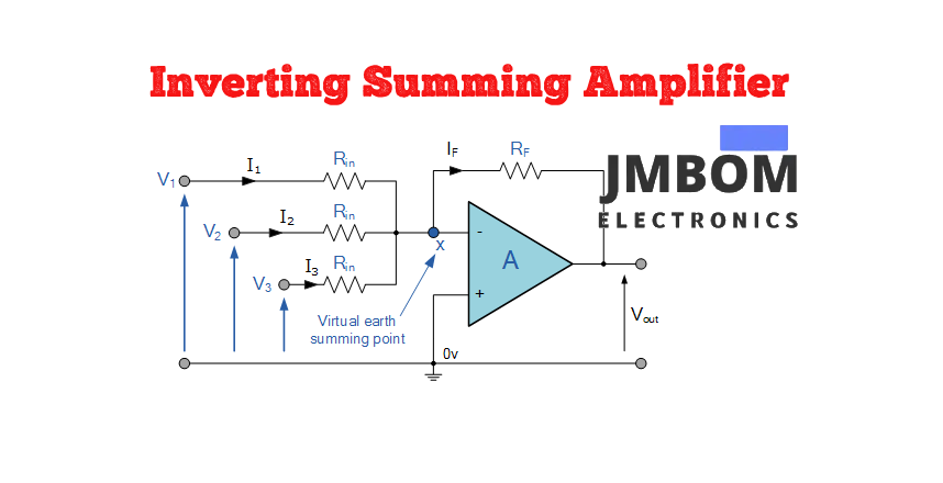
Inverting Summing Amplifier Circuit: Diagram and Output Equation
An inverting summing amplifier is essentially an expanded version of a basic inverting amplifier. In this configuration, multiple input signals are applied to the inverting input of the op-amp, while the non-inverting input is connected to ground. The resulting output is the inverted sum of all input voltages. The typical circuit layout is shown below.
Inverting Summing Amplifier Circuit
In this setup, grounding the non-inverting input causes the inverting input to sit at a virtual ground. This means the inverting input acts like a zero-voltage point, ideal for summing input currents from various sources.
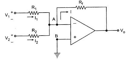
Output Equation of an Inverting Summing Amplifier
In the inverting summing amplifier circuit, all input signals are connected through individual resistors to the op-amp’s inverting input. The non-inverting input (often labeled as point B) is grounded. Due to the virtual ground principle, the inverting node (point A) also behaves as if it's at ground potential.
For a configuration with two or more input voltages, the output voltage can be calculated using the formula:
iniCopyEditVout = - (Rf/R1) * Vin1 - (Rf/R2) * Vin2 - ... - (Rf/Rn) * Vinn
Here:
- Rf is the feedback resistor.
- R1, R2, ..., Rn are the resistors connected to each input.
- Vin1, Vin2, ..., Vinn are the input voltages.
The negative sign indicates that the output is inverted relative to the sum of the input signals.
Inverting Summing Amplifier: Transfer Function Derivation & Practical Examples
Basic Current Relationships in the Circuit
Start with the virtual ground concept at the op-amp inputs:
VA = VB = 0 — (Equation I)
From the input side of the amplifier circuit:
- I₁ = (V₁ - VA) / R₁ = V₁ / R₁ — (Equation II)
- I₂ = (V₂ - VA) / R₂ = V₂ / R₂ — (Equation III)
At node A, the input current to the op-amp is approximately zero, so the total current at that node is:
- I = I₁ + I₂ — (Equation IV)
From the output side:
- I = (VA - Vo) / Rf = -Vo / Rf — (Equation V)
Now, substitute Equations II and III into Equation IV:
-Vo / Rf = V₁ / R₁ + V₂ / R₂
Multiply both sides by -Rf:
Vo = -Rf × (V₁ / R₁ + V₂ / R₂)
Or,
Vo = –[(Rf/R₁) × V₁ + (Rf/R₂) × V₂]
If all resistors are equal (R₁ = R₂ = Rf), then:
Vo = – (V₁ + V₂) — (Equation VI)
This means the circuit performs an inverted sum of the input signals. By choosing resistor values appropriately, you can achieve weighted summation, e.g., aV₁ + bV₂, for any number of inputs.
So, the inverting summing amplifier combines multiple input voltages and outputs their inverted, scaled sum—hence the name summing amplifier or adder circuit.
Deriving the Transfer Function of an Inverting Summing Amplifier
This amplifier adds input voltages together and inverts the result. The gain applied to each input depends on the ratio of the feedback resistor to each input resistor. For the basic configuration with two inputs:
Vout = – [V₁ × (Rf / R₁) + V₂ × (Rf / R₂)]
Let’s derive this step-by-step using the superposition theorem.
Step 1: Apply V₁, Set V₂ = 0
With V₂ grounded, and due to the high open-loop gain of the op-amp, the voltage at the inverting input is held close to 0V (virtual ground). This causes the output to move as needed to maintain balance:
If the output is 5V and the gain is 100,000, the input differential voltage would be:
Vd = 5V / 100,000 = 50 µV
The current through the feedback resistor Rf is:
If = Vout / Rf
Current through R₁ due to V₁ is:
I₁ = V₁ / R₁
Assuming an ideal op-amp (input bias current ≈ 0), Kirchhoff’s Current Law (KCL) at the inverting node gives:
If + I₁ + I₂ + Ib = 0
Since Ib ≈ 0 and I₂ = 0 (V₂ is grounded), we get:
Vout / Rf = – V₁ / R₁
Thus:
Vout₁ = – V₁ × (Rf / R₁)
Step 2: Apply V₂, Set V₁ = 0
Following the same logic, we get:
Vout₂ = – V₂ × (Rf / R₂)
Total Output:
By adding the individual outputs:
Vout = Vout₁ + Vout₂
Vout = – [V₁ × (Rf / R₁) + V₂ × (Rf / R₂)]
General Transfer Function (n inputs):
For n input signals:
Vout = – [V₁ × (Rf / R₁) + V₂ × (Rf / R₂) + ... + Vn × (Rf / Rn)]
Example 1: Two-Input Summing Amplifier
Given:
- Rf = 100 kΩ
- R₁ = R₂ = 10 kΩ
- Vinput₁ = 1V, Vinput₂ = 2V
Using the formula:
Vout = – (Rf/R₁ × V₁ + Rf/R₂ × V₂)
= – (100/10 × 1 + 100/10 × 2)
= – (10 + 20) = –30V
So, the output is –30V, representing the amplified and inverted sum of the inputs.
Note: Output can vary based on real-world factors like bandwidth, supply voltage limits, and load resistance.
Example 2: Three-Input Summing Amplifier
Given resistors:
- R₁ = 20 kΩ, R₂ = 10 kΩ, R₃ = 50 kΩ
- Rf = 100 kΩ
- V₁ = 100 mV, V₂ = 200 mV, V₃ = 300 mV
Calculate closed-loop gains:
- ACL₁ = – (Rf / R₁) = – (100k / 20k) = –5
- ACL₂ = – (Rf / R₂) = – (100k / 10k) = –10
- ACL₃ = – (Rf / R₃) = – (100k / 50k) = –2
Output voltage:
Vout = – [(5 × 0.1) + (10 × 0.2) + (2 × 0.3)]
= – [0.5 + 2.0 + 0.6] = –3.1V
So, the output is –3.1 volts, combining all three scaled input signals.
Advantages and Disadvantages of an Inverting Summing Amplifier
Advantages
- The summing junction of the amplifier operates at a virtual ground, which ensures that the settings and signals from each channel remain isolated. This minimizes interference between channels and allows for accurate summing, regardless of signal level.
- This configuration is especially useful in audio engineering, where it enables professionals to combine multiple audio inputs into a single output track. Each input can be adjusted independently without affecting the overall output.
- Due to the virtual ground at the inverting terminal, there is inherent isolation between input sources and the output, reducing the chances of crosstalk and maintaining signal integrity.
Disadvantages
- One of the main drawbacks is its relatively lower voltage gain when compared to a non-inverting summing amplifier, limiting its amplification range in certain applications.
- The design is more sensitive to noise, which can degrade the signal-to-noise ratio (SNR) and reduce output accuracy.
- As the number of inputs increases, circuit analysis and design complexity grow, making it more challenging to maintain performance.
- The output is inverted in polarity relative to the summed input signals, which may not be desirable in applications requiring phase accuracy.
Applications of Inverting Summing Amplifier
- This amplifier is ideal for inverting the polarity or phase of the output signal relative to the input, useful in applications requiring signal phase reversal.
- It is commonly used in audio summing circuits, where multiple signals are added together and phase-inverted at the output.
- Serves as a core component in signal mixers, especially in audio processing, where equal-gain signal addition is needed.
- Useful for introducing a DC offset to an AC signal, combining both in a controlled manner.
- With simple modifications, it can function as a differential amplifier, producing an output voltage equal to the difference between two input signals.
Summary
In summary, the inverting summing amplifier is a versatile op-amp configuration that not only combines multiple signals into one but also inverts their polarity. Thanks to its low output impedance, high input impedance, and the ability to easily configure gain through resistor selection, it’s widely used in practical systems like audio mixers, signal conditioners, and analog computing circuits.
The performance of this circuit largely depends on the operational amplifier used. When configured properly, it acts as an inverter or buffer, and its output is determined by the input voltages and the resistor values.
Frequently Ask Questions
What is an inverting summing amplifier?
An inverting summing amplifier—also called an adder circuit—produces an output voltage that represents the amplified, inverted sum of two or more input voltages. It’s commonly based on an inverting op-amp configuration, which means the output is negative with respect to ground when the inputs are positive.
What’s the difference between inverting and non-inverting summing amplifiers?
The key difference lies in where the input signal is applied:
- In an inverting summing amplifier, inputs are connected to the inverting (–) terminal, and the output is 180° out of phase with the input.
- In a non-inverting summing amplifier, inputs go to the non-inverting (+) terminal, and the output maintains the same phase as the input.
How does an op-amp function as an adder?
An op-amp can work as a summing circuit by connecting multiple input signals through resistors to the inverting input. Thanks to the concept of virtual ground, each input contributes independently to the output without affecting the others. The op-amp sums these currents and outputs their negative sum, scaled by the feedback resistor.
Why would you use an inverting amplifier?
An inverting amplifier is useful when a 180-degree phase shift is needed. This makes it ideal for:
- Signal inversion
- Phase-shift oscillator designs
- Mixing audio channels while inverting their polarity It also allows for precise gain control through resistor selection.
How does an op-amp act as an integrator?
An op-amp integrator is a circuit that performs mathematical integration on an input signal. It produces an output voltage that is proportional to the time integral of the input, making it useful in analog computers, waveform generators, and signal processing systems.
When should you use a non-inverting amplifier?
Use a non-inverting op-amp when you need to:
- Preserve the signal phase (no inversion)
- Maintain high input impedance
- Prevent loading on the signal source These are common in buffer circuits, voltage followers, and any application where signal integrity must be preserved.
What are the disadvantages of an inverting summing amplifier?
While versatile, inverting summing amplifiers have some drawbacks:
- They generally offer lower gain than non-inverting versions.
- They invert the signal, which may not be suitable for all applications.
- They can be more sensitive to noise, affecting accuracy.
- Adding more inputs increases design complexity and can affect performance.
Related Articles
Guide to Low Dropout (LDO) Regulators and How They Work
ESP32-S3 Development Board: Pinout Diagram, Key Features, Technical Specs
DS18B20 Waterproof Temperature Sensor: Overview, Operation, and Common Uses
BAT54A Schottky Diode: Pinout and Common Uses
Infineon ILD8150E LED Driver IC Overview
LF353N Op-Amp Explained: Pinout, Features, and How It Works
ADXL335 Accelerometer Sensor: Pinout, Specs, Features, and How It Works
Engine Coolant Temperature Sensor: Overview, Function & Circuit Design
Crankshaft Position Sensor: Overview, Circuit Function& Comparison with Camshaft Sensors

Christopher Anderson
Christopher Anderson has a Ph.D. in electrical engineering, focusing on power electronics. He’s been a Senior member of the IEEE Power Electronics Society since 2021. Right now, he works with the KPR Institute of Engineering and Technology in the U.S. He also writes detailed, top-notch articles about power electronics for business-to-business electronics platforms.
Subscribe to JMBom Electronics !


