


How to Use a Transistor as a Switch
Catalog
What Is a Transistor?Types of BJT TransistorsUsing a Transistor as a SwitchOperating Modes of TransistorsCut-off Region CharacteristicsTransistor as a Switch – NPNTransistor as a Switch – PNPSwitching Operation of a Darlington TransistorDarlington ConfigurationsCommon Practical Applications of a Transistor as a SwitchDC Motor Control (Driver) for High Voltage ApplicationsWhy Use a Transistor Instead of a Switch?Summary of Key Points When Using Transistors as SwitchesRelated ArticlesA key component in the electrical and electronics field is the control device that allows a small signal to regulate a much larger current—much like a valve that controls water flow from pumps or pipes. In earlier times, vacuum tubes served as these control devices. While vacuum tubes worked effectively, they were bulky, consumed a lot of power, and generated significant heat, which shortened their lifespan. To overcome these drawbacks, the transistor was invented, offering a compact, efficient, and reliable solution for the electrical and electronics industry. This groundbreaking device was created by William Shockley in 1947. In this article, we’ll explore what a transistor is, how to use it as a switch, and its key characteristics.
What Is a Transistor?
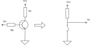
A transistor is a semiconductor device with three terminals that can be used for switching circuits and amplifying weak signals. In fact, thousands or even millions of transistors are interconnected on tiny integrated circuits (chips) to create computer memory and other complex electronics. When used as a switch, a transistor opens or closes a circuit, making it ideal for low-voltage applications due to its low power consumption. A transistor functions as a switch when operating in either the cutoff or saturation region.
Types of BJT Transistors
A basic transistor is made up of two PN junctions, formed by layering either N-type or P-type semiconductor material between two layers of the opposite type.
Types of Bipolar Junction Transistors (BJTs)
Bipolar junction transistors are mainly classified into two types:
- NPN
- PNP
A transistor has three terminals: the Base, the Emitter, and the Collector. The emitter is heavily doped and emits electrons into the Base region. The Base is lightly doped and passes these electrons on to the Collector. The collector is moderately doped and collects electrons from the Base.
An NPN transistor consists of two N-type semiconductor layers separated by a P-type layer, as shown above. Conversely, a PNP transistor is made up of two P-type layers separated by an N-type layer. Both NPN and PNP transistors operate on the same principle but differ in their biasing and power supply polarities.
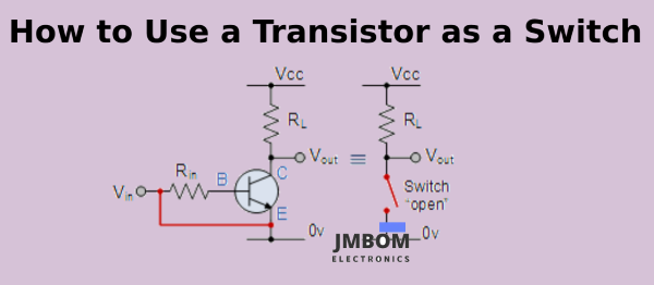
Using a Transistor as a Switch
When a BJT transistor is used as a switch, whether NPN or PNP, its biasing is set so that it operates at the extremes of its I-V characteristic curve. A transistor can work in three different modes: the active region, the saturation region, and the cutoff region. In the active region, the transistor functions as an amplifier. However, when used as a switch, it operates only in two modes — the saturation region (fully ON) and the cutoff region (fully OFF).
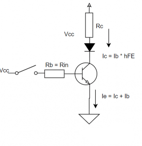
Below is the circuit diagram showing a transistor used as a switch:
Transistor as a Switch
Both NPN and PNP transistors can be used as switches. In some applications, a power transistor is directly used as a switch without the need for an additional signal transistor to drive it.
Operating Modes of Transistors
From the characteristic curves above, the pink-shaded area at the bottom represents the cutoff region, while the blue area on the left corresponds to the saturation region of the transistor. These regions are defined as follows:
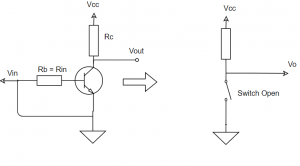
Cut-off Region
In the cut-off region, the transistor has zero base current (IB = 0), zero collector current (IC = 0), and the collector-emitter voltage (VCE) is at its maximum. This creates a large depletion region, preventing current from flowing through the device.
As a result, the transistor is considered to be fully OFF. For an NPN transistor used as a switch, the cut-off region means both junctions are reverse biased, with the base voltage (VB) less than about 0.7 V and collector current (IC) equal to zero. For a PNP transistor, the emitter must be at a lower (negative) potential relative to the base to achieve cutoff.
Cut-Off Mode
The cut-off region, or OFF mode, for a bipolar transistor used as a switch is defined by both junctions being reverse biased, collector current (IC) equal to zero, and the base voltage (VB) less than 0.7 V. In the case of a PNP transistor, the emitter voltage must be negative relative to the base terminal.
Cut-off Region Characteristics
In the cut-off region, the transistor exhibits the following characteristics:
- Both the base and input terminals are at 0 V (grounded).
- The base-emitter voltage is less than 0.7 V.
- The base-emitter junction is reverse biased.
- The transistor behaves like an open switch.
- When fully OFF, the transistor is in the cut-off region.
- The base-collector junction is also reverse biased.
- No current flows through the collector (IC = 0).
- The voltage at the collector-emitter junction, and at the output terminal, is high (logic ‘1’).
Saturation Region
In the saturation region, the transistor is biased with maximum base current (IB), allowing the maximum collector current to flow (IC = VCC / RL). This causes the collector-emitter voltage (VCE) to drop to a very low value, close to zero. At this point, the depletion layer shrinks to its smallest size, enabling maximum current to pass through the transistor. As a result, the transistor is fully switched ON.
Saturation Mode
Definition of Saturation Region (ON Mode)
When using a bipolar NPN transistor as a switch, the saturation region or ON mode is defined by both junctions being forward biased, collector current (IC) at its maximum, and the base voltage (VB) greater than 0.7 V. For a PNP transistor, the emitter voltage must be positive relative to the base. This is how a transistor operates as a switch.
Saturation Region Characteristics
The saturation region has the following features:
- Both the base and input terminals are connected to Vcc (typically 5 V).
- The base-emitter voltage is greater than 0.7 V.
- The base-emitter junction is forward biased.
- The transistor acts like a closed switch.
- When fully ON, the transistor enters the saturation region.
- The base-collector junction is also forward biased.
- Collector current is given by IC = Vcc / RL.
- The voltage across the collector-emitter junction, and at the output terminal, is approximately 0 V.
- A collector-emitter voltage near zero indicates ideal saturation.
Transistor as a Switch – NPN
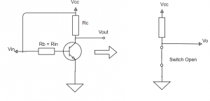
The switching action of an NPN transistor depends on the voltage applied to its base terminal. When the base-to-emitter voltage reaches about 0.7 V, the transistor switches ON, allowing current to flow freely from the collector to the emitter. In this state, the transistor acts like a closed switch, and the current flowing through the collector is considered the transistor current.
On the other hand, when no voltage is applied to the base, the transistor enters the cut-off region and behaves like an open circuit, meaning no current flows through the collector. In this switching setup, the load is connected to the transistor’s switching point, which serves as a reference. When the transistor switches ON, current flows from the power source, through the load, and then to ground.
NPN Transistor as Switch
To better understand this switching method, let’s look at an example.
Suppose a transistor has a base resistance of 50 kΩ, a collector resistance of 0.7 kΩ, and the applied voltage is 5 V. The transistor’s current gain (β) is 150. At the base terminal, a signal varying between 0 and 5 V is applied. This means the collector output will change depending on whether the input voltage is 0 V or 5 V. Refer to the diagram below.
When the collector-emitter voltage (VCE) is 0 (indicating saturation), the collector current (IC) is calculated as:IC=VCCRC=50.7=7.1 mAIC = \frac{V_{CC}}{R_C} = \frac{5}{0.7} = 7.1\, \text{mA}IC=RCVCC=0.75=7.1mA
Given the current gain β = 150, the base current (IB) is:IB=ICβ=7.1 mA150=47.3 μAI_B = \frac{I_C}{\beta} = \frac{7.1\, \text{mA}}{150} = 47.3\, \mu\text{A}IB=βIC=1507.1mA=47.3μA
So, the base current required to switch the transistor ON is approximately 47.3 microamperes.
Using the values above, the maximum collector current is 7.1 mA when the collector-emitter voltage is zero, and the corresponding base current is 47.3 µA. This shows that when the base current exceeds 47.3 µA, the NPN transistor enters the saturation region.
Now, let’s consider two input voltage cases:
- VC=VCC−(IC×RC)=5−0=5 VV_C = V_{CC} - (I_C \times R_C) = 5 - 0 = 5\, VVC=VCC−(IC×RC)=5−0=5V
- IB=Vi−VBERBI_B = \frac{V_i - V_{BE}}{R_B}IB=RBVi−VBEIB=5−0.750,000=56.8 μAI_B = \frac{5 - 0.7}{50,000} = 56.8\, \mu AIB=50,0005−0.7=56.8μA
This confirms that when the base current is above 56.8 µA (at 5 V input), the NPN transistor operates in the saturation region.
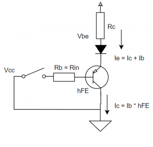
Transistor as a Switch – PNP
The switching operation of a PNP transistor is similar to that of an NPN transistor, with one key difference: in a PNP transistor, current flows from the emitter to the base. This configuration is typically used in circuits with a negative ground reference.
In a PNP transistor switch, the base is connected to a negative bias relative to the emitter. When the base voltage becomes sufficiently negative, base current flows, turning the transistor ON. If the base voltage is close to zero or less negative, the transistor behaves like an open circuit or presents very high impedance.
PNP Transistor as Switch
In this setup, the load is connected to the switching output and a reference point. When the PNP transistor is ON, current flows from the source, through the load, and then through the transistor to ground.
Just like with an NPN transistor, the input for a PNP transistor is applied at the base terminal. The emitter is connected to a fixed voltage, while the collector is connected to ground through a load. The circuit diagram below illustrates this setup.
In this configuration, the base is always negatively biased relative to the emitter. The base is connected to the negative side of the input voltage, and the emitter to the positive side. This means the base-to-emitter voltage is negative, while the emitter-to-collector voltage is positive. The transistor conducts when the emitter voltage is higher (more positive) than both the base and collector voltages. Therefore, the base voltage must be more negative than the other terminals for the transistor to switch ON.
To calculate the collector and base currents, we use the following relationships:IC=IE−IBI_C = I_E - I_BIC=IE−IBIC=β×IBI_C = \beta \times I_BIC=β×IB
whereIB=ICβI_B = \frac{I_C}{\beta}IB=βIC
Example
Suppose the load requires 120 mA and the transistor’s beta (current gain) is 120. The base current needed to saturate the transistor is:IB=ICβ=120 mA120=1 mAI_B = \frac{I_C}{\beta} = \frac{120\, \text{mA}}{120} = 1\, \text{mA}IB=βIC=120120mA=1mA
In practical situations, it’s common to provide 30–40% more base current to ensure proper saturation. This means the base current should be around 1.3 mA.
Switching Operation of a Darlington Transistor
Sometimes, the current gain of a single BJT transistor is too low to directly switch a load voltage or current. To overcome this, Darlington transistors are used. In this setup, a small transistor controls the switching ON and OFF, while a second transistor provides a much higher current gain to drive the output.
To increase the overall current gain, two transistors are connected in a “complementary gain compounding configuration.” In this arrangement, the total amplification is the product of the gains of the two individual transistors, resulting in much higher overall current gain.
Darlington Transistor
Darlington transistors typically consist of two bipolar transistors—one PNP and one NPN—connected so that the current gain of the first transistor is multiplied by the gain of the second.
This configuration makes the pair behave like a single transistor with a very high current gain, even with a very small base current. The total current gain (β) of a Darlington transistor is the product of the individual gains of the two transistors:β=β1×β2\beta = \beta_1 \times \beta_2β=β1×β2
Thanks to this high overall gain, Darlington transistors can handle much larger collector currents compared to a single transistor switch.
For example, if the first transistor has a gain of 100 and the second transistor has a gain of 50, the total current gain becomes:β=100×50=5000\beta = 100 \times 50 = 5000β=100×50=5000
So, if the load requires 200 mA, the base current needed for the Darlington transistor is:IB=200 mA5000=40 μAI_B = \frac{200\, \text{mA}}{5000} = 40\, \mu AIB=5000200mA=40μA
This is a huge reduction compared to the roughly 1 mA base current needed for a single transistor.
Darlington Configurations
There are two main types of Darlington transistor configurations:
In the typical Darlington switch configuration, the collector terminals of both transistors are connected together. The emitter of the first transistor is connected to the base of the second transistor. This means the current flowing out of the emitter of the first transistor becomes the input current for the second transistor, turning it ON.
The first transistor receives the input signal at its base terminal. It amplifies this signal and drives the second transistor. The second transistor further amplifies the current, resulting in a very high overall current gain. This is one of the key advantages of a Darlington transistor compared to a single BJT device.
Besides offering high current and voltage switching capabilities, Darlington transistors also provide faster switching speeds. This makes them ideal for applications such as inverter circuits, DC motor control, lighting systems, and stepper motor drives.
One important difference when using Darlington transistors instead of single BJTs as switches is the input voltage requirement. Because two PN junctions are connected in series, the base-to-emitte
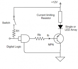
Common Practical Applications of a Transistor as a Switch
A transistor’s ability to control the collector current by varying the base current makes it ideal for switching applications. By turning the base current ON or OFF, the transistor acts like a switch controlling larger currents. Below are a few examples using an NPN transistor as a switch:
Light-Operated Switch
This circuit uses a transistor switch alongside a Light-Dependent Resistor (LDR) arranged in a voltage divider. When the environment is dark, the LDR’s resistance increases, causing the transistor to switch OFF and the bulb to remain unlit. In bright light, the LDR’s resistance decreases, increasing the base current to the transistor. This switches the transistor ON, allowing collector current to flow and lighting up the bulb.
Heat-Operated Switch
A key component in this circuit is the thermistor, a resistor whose resistance varies with temperature. When the temperature is low, the thermistor’s resistance is high; when heated, its resistance decreases. As the thermistor heats up, the base current of the transistor increases, boosting the collector current and triggering the siren. This setup is useful as a fire alarm system.
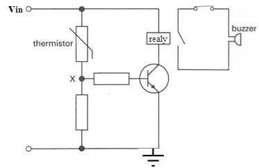
Heat-Operated Switch
DC Motor Control (Driver) for High Voltage Applications
When no voltage is applied to the transistor’s base, the transistor remains OFF and no current flows through it. As a result, the relay stays de-energized (OFF). In this state, power to the DC motor is supplied through the relay’s Normally Closed (NC) terminal, so the motor runs when the relay is OFF. When a high voltage is applied to the transistor’s base (for example, using a BC548 transistor), it switches ON, energizing the relay coil and controlling the motor accordingly.
Practical Example
Let’s calculate the base current and base resistor value required to fully turn ON a transistor when the load needs 200 mA and the input voltage is 5 V.
- Assume the transistor’s current gain (β) is 200.
Base current:IB=ICβ=200 mA200=1 mAI_B = \frac{I_C}{\beta} = \frac{200\, \text{mA}}{200} = 1\, \text{mA}IB=βIC=200200mA=1mA
Base resistor:RB=Vin−VBEIB=5 V−0.7 V1×10−3 A=4.3 kΩR_B = \frac{V_{in} - V_{BE}}{I_B} = \frac{5\, \text{V} - 0.7\, \text{V}}{1 \times 10^{-3}\, \text{A}} = 4.3\, k\OmegaRB=IBVin−VBE=1×10⁻³A5V−0.7V=4.3kΩ
Applications of Transistor Switches
Transistor switches are widely used for interfacing low-voltage control signals (like those from digital ICs or logic gates) with high-current or high-voltage devices such as motors, relays, and lights. For example, a logic gate output at +5 V can control devices that require 12 V or even 24 V power supplies.
Additionally, loads like DC motors often need speed control through continuous pulse signals. Transistor switches enable faster and more reliable switching than traditional mechanical switches, making them ideal for these applications.
Why Use a Transistor Instead of a Switch?
When using a transistor instead of a mechanical switch, even a very small base current can control a much larger current flowing through the collector terminal. Transistors are often used to drive relays and solenoids, where they act as electronic switches. For applications that require switching higher currents or voltages, Darlington transistors are preferred due to their much higher current gain.
Summary of Key Points When Using Transistors as Switches
- BJTs should be operated in either fully ON (saturation) or fully OFF (cut-off) states when used as switches.
- A small base current controls a much larger collector load current.
- When switching inductive loads like relays or solenoids, it’s important to use flyback (flywheel) diodes to protect the transistor from voltage spikes.
- For switching higher voltages or currents, Darlington transistors are the best choice.
This article has covered the basics of transistors, their operating regions, how they function as switches, their characteristics, and practical applications. A related topic worth exploring next is digital logic transistor switches — their working principles and circuit diagrams.
Related Articles
Top 8051 Microcontroller Projects for Engineering Students
How Fingerprint Sensors Work and Where They're Used
Arduino Sensors: Types and Uses
Arduino Relay Module: How It Works, Circuit Diagram & Code
Plug Flow Reactor (PFR): Function, Design Principles & Common Uses
PIC Microcontroller Programming for Your Electronics Project
Fiber Optic Sensors: Types and Real-World Uses
ADC (Analog-to-Digital Converter) Module in PIC Microcontrollers

Christopher Anderson
Christopher Anderson has a Ph.D. in electrical engineering, focusing on power electronics. He’s been a Senior member of the IEEE Power Electronics Society since 2021. Right now, he works with the KPR Institute of Engineering and Technology in the U.S. He also writes detailed, top-notch articles about power electronics for business-to-business electronics platforms.
Subscribe to JMBom Electronics !


