


Thin Film Transistor: Structure, Working, Connection & Applications
Catalog
What is a Thin Film Transistor?Working Principle of Thin Film Transistor (TFT)Structure of Thin Film Transistor (TFT)Materials Used in TFT LayersThin Film Transistor (TFT) Fabrication ProcessHow to Connect a Thin Film TransistorOperation of a Thin Film Transistor (TFT)Difference Between Thin Film Transistor (TFT) and MOSFETFrequently Ask QuestionsAdvantages and Disadvantages Frequently Ask QuestionsRelated ArticlesThe development of transistors by the Radio Corporation of America (RCA) laid the groundwork for thin film technology. In 1957, John Wallmark, a researcher at RCA, was granted the first patent related to thin film transistors (TFTs). Building on years of innovation in microelectronics and semiconductor fields, the Thin Film Transistor (TFT) officially emerged in 1962.
TFTs are a special class of transistors widely used in liquid crystal displays (LCDs) to enhance image quality—specifically improving contrast, brightness, and addressability. Unlike traditional MOSFETs, TFTs are fabricated using thin film layers on an insulating substrate, making them ideal for display technologies.
What is a Thin Film Transistor?
A Thin Film Transistor (TFT) is a type of Field-Effect Transistor (FET) designed for use in each individual pixel of an LCD screen. It enables fast switching, high contrast, and better brightness control in displays. Essentially, each pixel in a modern LCD has its own dedicated TFT to control its on/off state, contributing to sharper and more accurate visuals.
Definition: A TFT is a field-effect transistor fabricated by depositing thin films of active semiconductor material, dielectric layer, and metallic contacts over a supporting substrate, usually glass or plastic.
Working Principle of Thin Film Transistor (TFT)
A Thin Film Transistor operates as a tiny individual switch for each pixel in a display. When voltage is applied to the gate terminal, it modulates the current flow between the source and drain terminals. This process enables the pixel to turn on or off quickly and precisely, which is essential for rendering fast-changing images in displays.
In LCDs, TFTs are arranged in a matrix format (known as active matrix technology) where each pixel is actively controlled. This configuration significantly improves display performance in terms of response time, contrast ratio, and brightness.
TFTs are considered active components and are essential in various commercial and industrial display applications, such as:
- Digital radiography detectors
- Head-up displays (HUDs)
- Televisions
- Smartphones
- Computer monitors
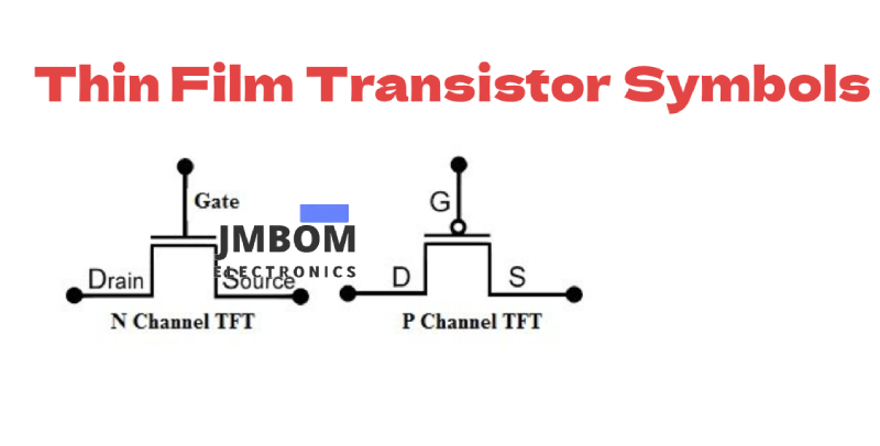
Structure of Thin Film Transistor (TFT)
A TFT is a type of Field-Effect Transistor (FET) that differs from conventional silicon-based transistors by using thin films of materials deposited on an insulating substrate (commonly glass or plastic).
The basic layers in a TFT structure include:
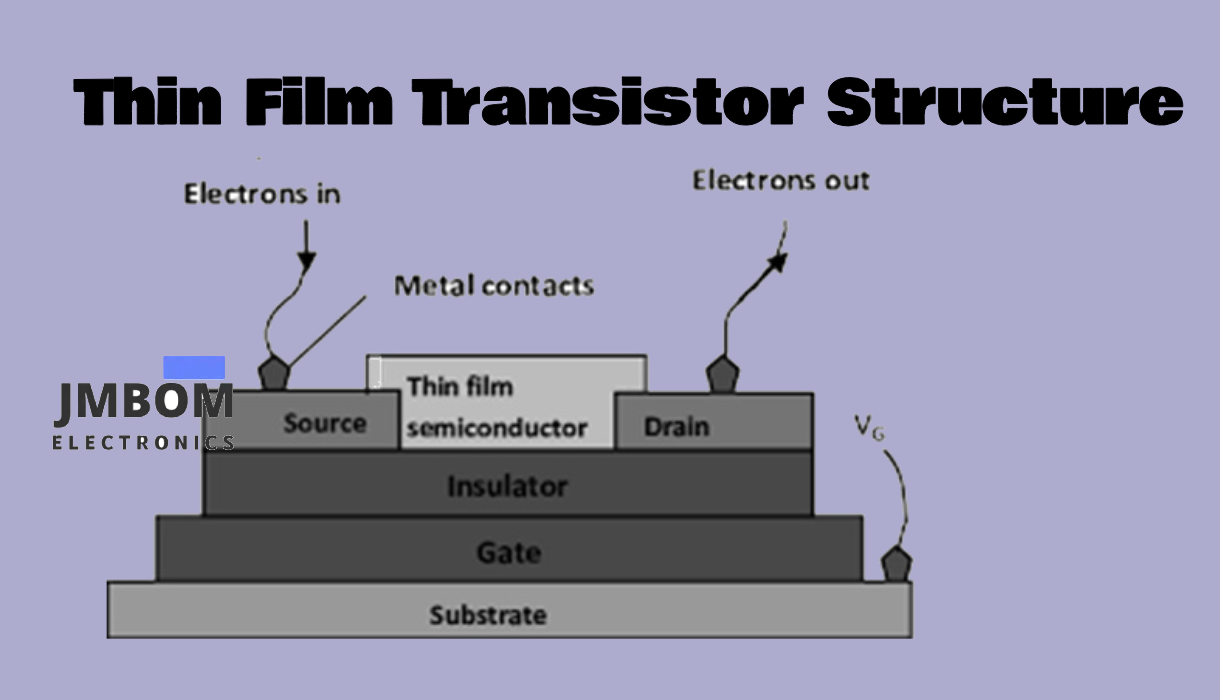
- Substrate (flexible or rigid, usually glass or plastic)
- Gate electrode (metal layer)
- Gate insulator (dielectric layer such as SiO₂)
- Semiconductor layer (often amorphous silicon or oxide semiconductors)
- Source and drain electrodes (metal contacts)
These layers are fabricated using deposition techniques such as chemical vapor deposition (CVD) or sputtering.
This multilayer structure allows the TFT to operate reliably with precise control over pixel states in large-area electronics.
Materials Used in TFT Layers
A Thin Film Transistor (TFT) consists of multiple thin layers, each made from specific materials chosen for their electrical, optical, or mechanical properties. These layers are stacked sequentially to form the complete device. The materials used in each layer are described below:
- Substrate Layer The bottom layer of a TFT is the substrate, which serves as the physical foundation for the entire device. It is typically made from materials like: Glass (a few microns thick) Metal foils Flexible polymers, such as Polyethylene Terephthalate (PET) The choice depends on whether the TFT is intended for rigid or flexible electronics.
- Gate Electrode The second layer is the gate electrode, which controls the flow of current between the source and drain. It is usually fabricated from conductive metals such as: Aluminum (Al) Gold (Au) Chromium (Cr) The selected material depends on the required conductivity, cost, and compatibility with other layers.
- Gate Insulator (Dielectric Layer) This insulating layer separates the gate electrode from the semiconductor to prevent electrical shorting. Common dielectric materials include: Silicon Dioxide (SiO₂) Silicon Nitride (Si₃N₄) This layer plays a crucial role in maintaining electrical isolation and influencing the device’s threshold voltage.
- Semiconductor Layer The active layer that carries charge is usually made of: Amorphous Silicon (a-Si) Polycrystalline Silicon Metal-oxide semiconductors (e.g., IGZO – Indium Gallium Zinc Oxide) This layer determines the electrical switching behavior of the TFT.
- Source and Drain Electrodes The electrodes that inject and collect carriers from the semiconductor are formed using highly conductive materials such as: Silver (Ag) Chromium (Cr) Aluminum (Al) Gold (Au) Indium Tin Oxide (ITO) – a transparent conductor often used in display applications These electrodes are patterned over the semiconductor to enable current flow when the device is active.
- Encapsulation Layer Finally, the entire structure is protected by an encapsulation layer, which can be made from: Ceramic materials Polymer coatings This layer provides mechanical protection and shields the device from moisture and contaminants.
Thin Film Transistor (TFT) Fabrication Process
The fabrication of a Thin Film Transistor involves sequential deposition of multiple layers on a substrate, using various deposition and patterning techniques. The steps are as follows:
- Substrate Preparation The process begins with thorough cleaning of the substrate—typically glass, metal foil, or flexible polymer. This is done using chemical treatments (acids or bases) to remove dust, organic contaminants, and residues to ensure good adhesion for subsequent layers.
- Gate Electrode Deposition After cleaning, metallic gate electrodes are deposited on the substrate. Thermal evaporation is commonly used for metals like aluminum, gold, or chromium. In the case of ceramic or polymer-based gates, techniques like inkjet printing or dip coating may be used.
- Gate Insulator Deposition The insulating dielectric layer is then deposited over the gate electrode to isolate it from the semiconductor layer. This step typically uses: Chemical Vapor Deposition (CVD) Plasma Enhanced Chemical Vapor Deposition (PECVD) Materials such as SiO₂ or Si₃N₄ are commonly used here.
- Semiconductor Layer Deposition Next, a semiconducting layer (e.g., amorphous silicon or IGZO) is applied: Dip coating or spray coating is used for solution-based or polymer semiconductors. For silicon-based layers, CVD is more common.
- Source and Drain Electrode Deposition The source and drain contacts are deposited on top of the semiconductor layer using methods similar to the gate electrode: Thermal evaporation for metals. Spray coating or dip coating for solution-processable conductors like Indium Tin Oxide (ITO). Proper masking techniques are used to define the electrode regions accurately.
- Encapsulation (Optional) To protect the completed TFT structure from moisture and environmental damage, a final encapsulation layer of polymer or ceramic is applied.
How to Connect a Thin Film Transistor
The basic operation of a TFT depends on the type of semiconductor used (n-type or p-type). Below is a general guideline for connecting and biasing a p-type TFT:
Thin Film Transistor Connection
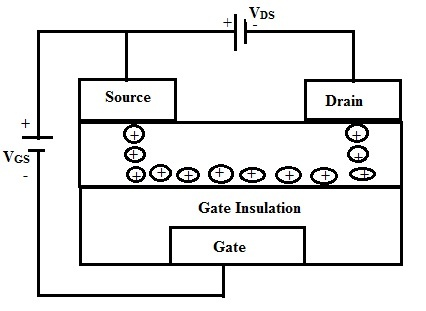
- Gate (G) controls the channel between the Source (S) and Drain (D).
- To turn on the transistor, a negative voltage (V_DS) is applied between Drain and Source.
- The Gate voltage (V_G) modulates the conductivity of the semiconducting channel. For p-type TFTs: A negative gate voltage enhances conduction. For n-type TFTs: A positive gate voltage is required.
Note: If the TFT uses n-type semiconductors, the bias voltages (V_G and V_DS) must be reversed.
In a matrix display, each TFT is connected to one pixel and driven by row (gate) and column (source/drain) lines. This allows precise control over each pixel’s on/off state.
Operation of a Thin Film Transistor (TFT)
The basic principle of TFT operation revolves around controlling the current flow between the source and drain terminals using a gate voltage.
- When the TFT is OFF: If no gate voltage is applied (or the gate-source voltage VGSV_{GS}VGS is zero or below the threshold), no conductive channel is formed in the semiconductor layer. As a result, no charge carriers (such as holes or electrons) accumulate between the source and drain terminals, and no current IDI_DID flows through the device.
- When the TFT is ON: To switch the transistor ON, a negative gate-to-source voltage (VGSV_{GS}VGS) is applied (in the case of a p-type TFT). This negative bias attracts holes (positive charge carriers) toward the gate insulator-semiconductor interface, forming a conductive channel. Once the channel is established, current (IDI_DID) can flow from drain to source when a drain-to-source voltage (VDSV_{DS}VDS) is also applied.
Note: For n-type TFTs, a positive VGSV_{GS}VGS is applied to attract electrons instead of holes.
Difference Between Thin Film Transistor (TFT) and MOSFET
| Aspect | Thin Film Transistor (TFT) | MOSFET |
|---|---|---|
| Full Form | TFT stands for Thin Film Transistor. | MOSFET stands for Metal-Oxide-Semiconductor Field-Effect Transistor. |
| Structure | A type of FET where the conductive channel is formed by depositing thin semiconductor films over an insulating substrate (e.g., glass or plastic). | A type of FET where a thin silicon oxide layer is placed between the gate and the semiconducting channel on a silicon wafer. |
| Semiconductor Materials | Made using various materials like cadmium selenide, zinc oxide (ZnO), amorphous silicon, or organic semiconductors. | Typically fabricated with materials like silicon (Si), silicon carbide (SiC), polysilicon, and high-k dielectrics. |
| Function | Acts as an individual pixel switch in LCDs, enabling high-speed ON/OFF control of display pixels. | Used for switching and amplifying signals in a wide variety of analog and digital circuits. |
| Applications | Mainly used in display technologies such as LCDs, OLEDs, and flat-panel displays. | Widely used in automotive systems, industrial electronics, power supplies, and communication circuits. |
Frequently Ask Questions
How is a Thin Film Transistor Different from a Normal Transistor?
Thin Film Transistors (TFTs) differ from normal transistors (typically bipolar junction transistors, or BJTs) in several ways, including their construction, materials, terminals, and functions.
1. Material Composition
- Normal Transistor: Usually made from high-purity silicon (Si) or germanium (Ge).
- TFT: Made using thin films of materials such as amorphous silicon, zinc oxide (ZnO), or cadmium selenide (CdSe) deposited on an insulating substrate like glass or plastic.
2. Terminal Configuration
- Normal Transistor: Has three terminals—Emitter, Base, and Collector.
- TFT: Also has three terminals, but named Source, Gate, and Drain, similar to a Field-Effect Transistor (FET).
3. Operation Principle
- Normal Transistor (BJT): Operates based on current control—a small current at the base controls a larger current between collector and emitter.
- TFT: Operates on voltage control—a voltage applied to the gate controls current flow between source and drain.
4. Function
- Normal Transistor: Functions as a switch or an amplifier in analog and digital circuits.
- TFT: Primarily used as a switch, especially in display applications, to turn pixels on and off rapidly.
5. Applications
- Normal Transistor: Common in audio amplifiers, signal processing, power electronics, and control circuits.
- TFT: Used in LCDs, OLED displays, flat-panel screens, and imaging sensors.
Advantages and Disadvantages
Advantages of Thin Film Transistors (TFTs)
- Low Power Consumption TFTs are energy-efficient, especially when displaying static images, making them ideal for portable electronic devices.
- Fast Response Time They switch pixels on and off rapidly, enabling smooth video playback and quick screen refresh rates.
- Essential for Modern Displays TFTs are the core technology behind LCDs, OLEDs, and other flat-panel displays, offering precise control of individual pixels.
- Flexible Electronics Compatibility TFTs can be fabricated on low-cost, flexible substrates, making them suitable for bendable and wearable devices.
- High Accuracy and Sharpness TFT-based displays deliver high resolution, clear images, and accurate color reproduction.
- Superior Display Design Devices using TFTs are known for their sleek and thin form factor, allowing for compact and elegant product designs.
- Reduced Eye Strain The improved brightness, contrast, and clarity of TFT screens help minimize eye fatigue during prolonged use.
Disadvantages of Thin Film Transistors (TFTs)
- Requires Backlighting TFT displays do not emit light on their own and rely on LED backlighting, which adds complexity and power consumption.
- Limited Flexibility with Glass Substrates Many TFTs are still built on glass panels, which are rigid and limit their use in flexible or curved display applications.
- Visibility Dependent on Backlight TFT screens are not readable unless the LED backlight is active, affecting visibility in extremely bright or low-power conditions.
- Higher Battery Drain Compared to some other display technologies (e.g., e-ink or OLED in certain modes), TFTs can drain batteries faster, especially in high-brightness use.
Applications of Thin Film Transistors (TFTs)
Thin Film Transistors are widely used in modern electronics, particularly in display technologies and sensing systems. Their ability to control individual pixels and operate at high speeds makes them essential in many applications.
Key Applications Include:
- Display Technology TFT LCDs (Thin-Film Transistor Liquid Crystal Displays) are the most prominent use case. Commonly found in smartphones, laptops, computer monitors, and flat-panel televisions. Also used in projectors, digital cameras, and navigation systems.
- Consumer Electronics Found in video game systems, handheld gaming devices, and personal digital assistants (PDAs). Integrated into dashboard displays and infotainment systems in automobiles.
- Advanced Display Systems Used in emerging technologies like OLED displays and flexible/organic electronics. Employed in e-paper displays and wearable devices due to their thin, lightweight structure.
- Sensors and Imaging Serve as active elements in X-ray detectors, especially in digital radiography and medical imaging. Used in chemical and biological sensors for various industrial and healthcare applications.
- Materials Research and Development TFTs play a major role in materials chemistry and thin-film device research, offering platforms for testing new semiconducting and dielectric materials.
Conclusion
In summary, the Thin Film Transistor (TFT) is a vital component in modern digital display systems and flexible electronics. Compared to conventional MOSFETs, TFTs offer faster response times, high pixel control, and the ability to be fabricated on low-cost, flexible substrates. As technology progresses, researchers are continuously developing next-generation TFT devices with improved performance, transparency, and flexibility.
Frequently Ask Questions
What is a Thin-Film Transistor (TFT)?
A Thin-Film Transistor (TFT) is a type of Field-Effect Transistor (FET) that is built using thin layers of semiconductor and insulating materials, deposited on an insulating substrate like glass or plastic. It acts as an electronic switch, commonly used to control individual pixels in displays such as LCDs.
What is the Difference Between FET and TFT?
- A FET is a broad category of transistor where current is controlled by an electric field.
- A TFT is a special type of FET made using thin films deposited on an insulating base.
Think of it like this: All TFTs are FETs, but not all FETs are TFTs.
What is the Function of a Thin Film?
Thin films serve many purposes across various technologies:
- In electronics, they are used in transistors, sensors, and circuits.
- In photovoltaics, they form the basis of solar cells.
- In data storage, thin films are used for magnetic coatings.
- They also help reduce material usage while enhancing performance compared to bulk materials.
Why Do We Need Thin Film Technology?
- Cost-effective: Requires less material than bulk.
- Improves device performance: Enhances electrical, optical, or magnetic properties.
- Essential for miniaturization: Enables the creation of smaller, more powerful, and more efficient electronic devices.
- Critical in emerging technologies: Used in flexible displays, solar panels, MEMS, and advanced sensors.
Which is Better: FET or MOSFET?
- FETs (including JFETs and MESFETs) are generally used in analog circuits due to their low noise and simplicity.
- MOSFETs (a type of FET using an oxide layer) dominate digital circuits because of their high speed, scalability, and integration density.
So: FET = better for analog MOSFET = better for digital
What’s the Difference Between EFT and TFT (Tapping)?
This refers to psychological techniques, not electronics:
- TFT (Thought Field Therapy) uses tapping to balance the body's energy.
- EFT (Emotional Freedom Technique) combines tapping with affirmations to reduce emotional distress.
Note: This "TFT" is unrelated to Thin-Film Transistors.
Why Do We Want Smaller Transistors?
Smaller transistors allow:
- More transistors per chip
- Faster processing speeds
- Lower power consumption
- Smaller, more powerful devices This principle is what drove Moore’s Law—the idea that the number of transistors on a chip doubles every two years.
What is a Thin Film (in Simple Words)?
A thin film is a very thin layer of material—just a few nanometers to micrometers thick—that spreads across a surface. It's like a skin of metal, semiconductor, or plastic that’s used to build tiny, high-performance electronics.
Related Articles
Iron Core Inductor : Construction, Formula, Working & Its Applications
Air Core Inductors: Design, Operation, Inductance, and Common Uses
Logic Analyzers: Overview, Function, Types, Comparison & Maintenance
Passive High-Pass Filter: Overview, Circuit Design, Operation & Types
ESP32-S3 vs ESP32: What’s the Difference?
Chemical Sensors: Design, Operation, Types and Comparison with Biosensors

Christopher Anderson
Christopher Anderson has a Ph.D. in electrical engineering, focusing on power electronics. He’s been a Senior member of the IEEE Power Electronics Society since 2021. Right now, he works with the KPR Institute of Engineering and Technology in the U.S. He also writes detailed, top-notch articles about power electronics for business-to-business electronics platforms.
Subscribe to JMBom Electronics !


