
Nexperia USA Inc. BSS87,115


- Part Number:
BSS87,115
- Manufacturer:
- Category:
- RoHs:
 RoHS Compliant
 - Datasheet:
 BSS87,115_Datesheet
 - Description:
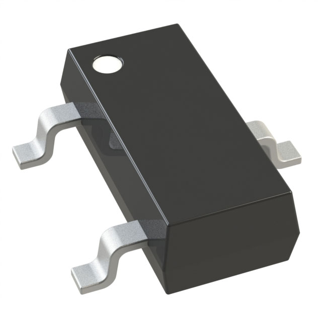
MOSFET N-CH 200V 400MA SOT89
- In stock 217,892

BSS87 Product Summary
Basic Information
- Part Number: BSS87
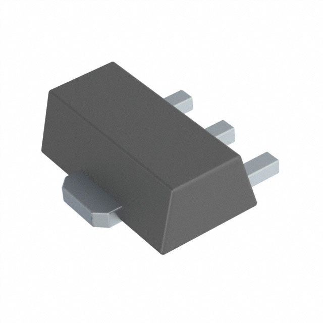
- Package Type: SOT89 (SC-62)
- Shipping Quantity: Not specified in the provided document
General Description
The BSS87 is an N-channel enhancement mode vertical Double-Diffused Field-Effect Transistor (DMOSFET) designed for medium power applications. It is housed in a SOT89 (SC-62) medium power and flat lead Surface-Mounted Device (SMD) plastic package. This transistor is suitable for automotive, industrial, computing, consumer, and wearable application markets.
Features and Benefits
- Direct Interface: Compatible with Complementary (C-MOS) transistor and Transistor-Transistor Logic (TTL) devices.
- Fast Switching: Very fast switching capabilities.
- No Secondary Breakdown: Enhanced reliability and performance.
Applications
- Relay Driver: Suitable for driving relays.
- High-Speed Line Driver: Ideal for high-speed line driving applications.
- Load-Side Loadswitch: Effective as a load-side load switch.
- Switching Circuits: General-purpose switching applications.
Quick Reference Data
- Drain-Source Voltage (VDS): 200 V
- Gate-Source Voltage (VGS): ±20 V (T = 25 °C)
- Drain Current (ID):Continuous: 0.4 A (VGS = 10 V, Tamb = 25 °C)Pulsed: 0.7 A (VGS = 10 V, Tamb = 25 °C, t ≤ 5 s)
- On-State Resistance (RDS(on)):1.6 to 3 Ω (VGS = 10 V, ID = 0.4 A, T = 25 °C)3.7 to 7 Ω (VGS = 10 V, ID = 0.4 A, T = 150 °C)
Pinning Information
- Pin 1 (S): Source
- Pin 2 (D): Drain
- Pin 3 (G): Gate
Ordering Information
- Package Type: SOT89 plastic surface-mounted package with die pad for good heat transfer; 3 leads.
Marking
- Marking Code: KA
Limiting Values
- Drain-Source Voltage (VDS): 200 V
- Gate-Source Voltage (VGS): ±20 V (T = 25 °C)
- Drain Current (ID):Continuous: 0.4 A (VGS = 10 V, Tamb = 25 °C)Pulsed: 1.6 A (Tamb = 25 °C, single pulse, tp ≤ 10 µs)
- Total Power Dissipation (Ptot):0.58 W (Tamb = 25 °C)1 W (Tsp = 25 °C)12.5 W (T = 25 °C)
- Junction Temperature (Tj): -55 to 150 °C
- Ambient Temperature (Tamb): -55 to 150 °C
- Storage Temperature (Tstg): -65 to 150 °C
- Source Current (IS): 0.4 A (Tamb = 25 °C)
Thermal Characteristics
- Thermal Resistance (Rth(j-a)):190 to 216 K/W (in free air)105 to 125 K/W (mounted on FR4 PCB, single-sided copper, tin-plated, mounting pad for drain 1 cm²)
- Thermal Resistance (Rth(j-sp)): 6 to 10 K/W
- Transient Thermal Impedance (Zth(j-a)): See Figures 4 and 5 for typical values.
Characteristics
- Static Characteristics:Drain-Source Breakdown Voltage (V(BR)DSS): 200 V (ID = 250 µA, VGS = 0 V, Tj = 25 °C)Gate-Source Threshold Voltage (VGSth): 0.8 to 2.8 V (ID = 1 mA, VDS = VGS, T = 25 °C)Drain Leakage Current (IDSS): 200 nA (VDS = 60 V, VGS = 0 V, Tj = 25 °C)Gate Leakage Current (IGSS): ±100 nA (VGS = ±20 V, VDS = 0 V, Tj = 25 °C)On-State Resistance (RDS(on)):1.6 to 3 Ω (VGS = 10 V, ID = 0.4 A, T = 25 °C)3.7 to 7 Ω (VGS = 10 V, ID = 0.4 A, T = 150 °C)Forward Transconductance (gfs): 0.8 S (VDS = 25 V, ID = 0.4 A, Tj = 25 °C)
- Dynamic Characteristics:Total Gate Charge (QG(tot)): 5.5 to 10 nCGate-Source Charge (QGS): 0.3 nCGate-Drain Charge (QGD): 1.4 nC (VDS = 50 V, ID = 0.25 A, VGS = 10 V, T = 25 °C)Input Capacitance (Ciss): 100 to 120 pFOutput Capacitance (Coss): 20 to 30 pFReverse Transfer Capacitance (Crss): 10 to 15 pF (VDS = 25 V, f = 1 MHz, VGS = 0 V, T = 25 °C)Turn-On Delay Time (td(on)): 2.7 to 6 nsRise Time (tr): 3.7 to 6 nsTurn-Off Delay Time (td(off)): 16.4 to 30 nsFall Time (tf): 7.5 to 20 ns (VDS = 50 V, ID = 0.25 A, VGS = 10 V, RG(ext) = 6 Ω, Tj = 25 °C)
- Source-Drain Diode:Source-Drain Voltage (VSD): 0.8 to 1.2 V (IS = 0.4 A, VGS = 0 V, Tj = 25 °C)
Package Outline
- Package Type: SOT89 (SC-62)
- Dimensions: See Figure 18 for detailed dimensions.
Soldering Information
- Reflow Soldering Footprint: See Figure 19 for dimensions.
- Wave Soldering Footprint: See Figure 20 for dimensions.
Revision History
- BSS87 v.5 (2014-12-09): Corrections to Figure 3.
- BSS87 v.4 (2014-08-15): No specific changes mentioned.
- BSS87 v.3 (2001-05-18): No specific changes mentioned.
- BSS87 v.2 (1997-06-23): Initial release.
Purchase
No need to register to order from JMBom Electronics, but signing in lets you track your order like a pro. Give it a try for a smoother shopping ride.
Means
Easy peasy! Pay your way with PayPal, Credit Card, or wire transfer in USD. We've got you covered.
RFQ(Request for Quotations)
Get the freshest prices and stock updates by asking for a quote! Our sales team will shoot you an email within a day. It's that simple.
IMPORTANT NOTICE
1. Look out for your order details in your inbox! (If it's missing, check the spam folder just in case.)
2. Our sales manager will double-check the order and keep you posted on any price or stock changes. No worries, we've got you covered.

Shipping Rate
We ship orders once a day around 5 p.m., except Sunday. Once shipped, the estimated delivery time depends on the courier company you choose, usually 5-7 working days.

Shipping Methods
We provide DHL, FedEx, UPS, EMS, SF Express, and Registered Air Mail international shipping.


Payment
You can pay the orders on the website directly or pay by wire transfer offline. We support: Paypal、VISA、Credit Card.


Nexperia USA Inc.
Nexperia USA Inc.
Nexperia USA Inc.
Nexperia USA Inc.
Nexperia USA Inc.
Nexperia USA Inc.
Nexperia USA Inc.
Nexperia USA Inc.
Nexperia USA Inc.

Nexperia USA Inc.
Nexperia USA Inc.
Nexperia USA Inc.