


What is a Step Recovery Diode? – Working Principle & Applications
Catalog
What is a Step Recovery Diode?Step Recovery Diode ConstructionStep Recovery Diode: Working Principle & CharacteristicsStep Recovery Diode CircuitDifferent IC PackagesAdvantagesDisadvantagesApplicationsRelated ArticlesDiodes are simple yet highly versatile electronic components, available in a wide range of types to suit various application requirements. Each diode type features unique characteristics tailored to specific uses.
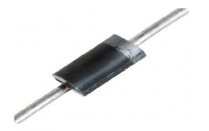
One relatively uncommon but exceptionally useful type is the Step Recovery Diode (SRD), also referred to as a charge-storage diode, snap-off diode, or memory varactor. This article provides a concise overview of the Step Recovery Diode (SRD).
What is a Step Recovery Diode?
A step recovery diode, or SRD, is a semiconductor diode specifically designed to generate extremely short-duration pulses.
It offers extremely fast switching speeds at low frequencies, which also makes it suitable for use as a charge-controlled switch.
This type of diode is capable of producing very sharp, well-defined pulses.
The circuit symbol for the step recovery diode is shown below.
Step Recovery Diode
At low frequencies, the step recovery diode operates in a similar manner to a conventional diode. When forward-biased, it conducts current, and when reverse-biased, it behaves as an open circuit. However, when the diode is switched from forward bias to reverse bias, its state changes very rapidly. At high frequencies, this switching transition does not occur instantaneously.
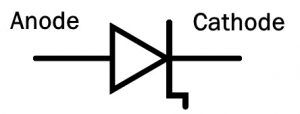
SRD Symbol
Step Recovery Diode Construction
The construction of a step recovery diode is similar to that of a conventional diode, with the key difference lying in its doping concentration. The doping level near the PN junction is relatively low.
The basic structure of an SRD is derived from the Shockley diode, featuring two PN junctions connected in series, plus a third terminal for the input voltage. This gives it unique dynamic switching characteristics not found in standard single-PN-junction diodes.
Owing to the lower number of charge carriers in the junction region, this structure achieves an extremely short switching time, on the order of just a few nanoseconds. With a lower charge density in the junction region, the residual charge can be removed rapidly when the diode transitions from forward bias to reverse bias.
The diagram below illustrates the doping profile of the step recovery diode.
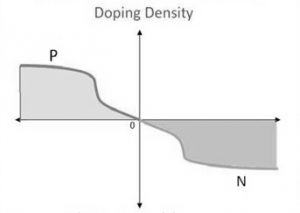
Step Recovery Diode Construction
At low frequencies, the step recovery diode behaves much like a conventional diode. It exhibits very low impedance—approximately 1 ohm—but its impedance gradually increases as charge accumulates at the junction.
When the input enters its negative cycle, the charge carriers require a short time to fully dissipate from the junction. As a result, a small current can be detected at the beginning of the negative input cycle.
Step Recovery Diode: Working Principle & Characteristics
Step recovery diodes (SRDs) are widely used for repetitive pulsed operation, thanks to their exceptional performance in high-speed switching scenarios. A key feature of these diodes is their extremely fast recovery time, which enables them to handle high peak currents and voltages. They are also commonly referred to as charge-storage diodes (due to their charge retention capability) or snap-off diodes, but it is important to note they are not avalanche diodes—these are distinct device types with different operating mechanisms.
Like many semiconductor devices, step recovery diodes have junction capacitance, which must be charged before the diode can conduct. The junction capacitance of SRDs is relatively large, meaning it requires a certain amount of time to charge to a level that allows normal current conduction. This capacitance is formed by the depletion region between the two PN junctions in the SRD’s structure.
When a reverse bias voltage is applied across the diode, the junction capacitance charges gradually until it reaches a critical threshold. Unlike avalanche diodes, SRDs do not rely on avalanche breakdown for conduction. Instead, once the stored charge in the junction is depleted, the diode transitions rapidly from a conducting state to a non-conducting state.
A defining characteristic of SRDs is that once the stored charge is fully dissipated, the reverse current drops to zero abruptly—this eliminates the reverse current tailing that is common in conventional diodes. Additionally, SRDs exhibit very fast fall times and excellent forward conductivity.
Due to their strong forward conductivity, SRDs can store a large number of minority charge carriers when forward-biased. The forward bias characteristics of an SRD are similar to those of a conventional diode. It is this ability to store significant amounts of minority charge carriers during forward operation that gives the SRD its alternative name: the charge-storage diode.
These devices exhibit a negative resistance characteristic, meaning they carry more current as the applied voltage decreases.
To better understand how Step Recovery Diodes function, we first need to grasp the concept of negative resistance. This phenomenon occurs when current flowing through a device causes its voltage to drop, rather than rise as it does in most components. Under these conditions, a negative voltage can be generated and utilized as energy.
This behavior enables the diodes to operate as amplifiers or oscillators in specific circuit configurations. At low frequencies, the diode behaves like a conventional diode: it conducts once forward‑biased. Compared with other diodes, it has a lower doping level.
Step Recovery Diode Circuit
Below is an implementation of an SRD (step recovery diode)‑based UWB pulse generator circuit. In typical UWB (ultra‑wideband) wireless communications and carrier‑free UWB radar systems, sub‑nanosecond or narrow nanosecond pulses are used as the transmission medium. This circuit is therefore designed to generate pulses at the sub‑nanosecond level. The circuit can be constructed using a resistor R, an SRD, and a load resistor RL.
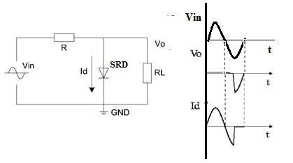
UWB Pulse Generator Circuit with SRD
The operating principle of this circuit relies on the abrupt step-recovery characteristic of the SRD to generate the drive pulse, reduce rise time, and narrow the pulse width, thereby producing the required UWB pulse.
The final measured pulse width is approximately 600 ps at an amplitude of 5 V, which is sufficient for most practical applications.
However, the circuit exhibits excessive noise and a relatively low output amplitude.
The input and output waveforms of this circuit are shown in the diagram above.
Different IC Packages
Step recovery diodes (SRDs) are available in a variety of IC packages, including:
- DO (Diode Outline)
- SOD (Small Outline Diode)
- TO (Transistor Outline)
- SOT (Small Outline Transistor)
- DPAK (Discrete Package)
- MELF (Metal Electrode Leadless Face)
- For step recovery diodes, MELF packages primarily include MicroMELF, QuadroMELF, and MiniMELF.
- Large surface‑mount packages such as D2PAK incorporate an integrated heat sink.
- SC-74, SC-76, and SC-59 are plastic, surface‑mount packages with three terminals.
- Powermite®3 is a compact, high‑power‑density surface‑mount rectifier package with low thermal resistance.
Advantages
The key advantages of step recovery diodes include:
- Faster forward current conduction compared to conventional diodes
- Short switching time and fast response
- Ability to generate extremely sharp pulses, ideal for pulse generators
- High efficiency and simple design
- Fast transient response
- Low cost
- Low power loss and short reverse recovery time
Disadvantages
Some limitations of step recovery diodes are:
- Switching speed decreases with increasing frequency
- Not suitable for very high‑frequency operation
- Lower efficiency when the input‑output differential is large
- May require a heat sink
- Only capable of step‑down operation
Applications
Typical applications for step recovery diodes include:
- High‑speed pulse shaping
- Frequency multipliers and high‑frequency harmonic generators
- Microwave frequency multiplication with high efficiency, up to approximately 20× multiplication factor
- Parametric amplifiers and pulse generators
- Voltage‑controlled oscillators (VCOs)
- Frequency synthesizers, comb generators, and sampling phase detectors
- Microwave and RF electronics
- In summary, the step recovery diode (SRD) is a specialized semiconductor diode used to generate extremely sharp pulses, making it widely used in microwave and radio‑frequency applications.
Here is a question for you: What is a Drift Step Recovery Diode (DSRD)?
Related Articles
Diode Dynamics: Real-World Behavior in Fast Power and RF Circuits

Christopher Anderson
Christopher Anderson has a Ph.D. in electrical engineering, focusing on power electronics. He’s been a Senior member of the IEEE Power Electronics Society since 2021. Right now, he works with the KPR Institute of Engineering and Technology in the U.S. He also writes detailed, top-notch articles about power electronics for business-to-business electronics platforms.
Subscribe to JMBom Electronics !


