


Diode-Transistor Logic (DTL): Circuit Design,Truth Table, and Applications
Catalog
What Is Diode-Transistor Logic (DTL)?Diode-Transistor Logic CircuitHow Diode-Transistor Logic (DTL) WorksTruth Table for Diode-Transistor Logic (DTL)Propagation Delay in Diode-Transistor Logic (DTL)Modified Diode-Transistor Logic CircuitWorking of the Modified Diode-Transistor Logic (DTL) CircuitSummary of Logic OperationApplications of the Modified DTL CircuitComparison Between DTL, TTL, and RTL Logic FamiliesAdvantages of Diode-Transistor Logic (DTL)Disadvantages of Diode-Transistor LogicApplications of Diode-Transistor LogicFrequently Ask QuestionsRelated ArticlesThere are several logic families used in the design of digital circuits, including Resistor-Transistor Logic (RTL), Emitter-Coupled Logic (ECL), Diode-Transistor Logic (DTL), Complementary Metal-Oxide-Semiconductor (CMOS), and Transistor-Transistor Logic (TTL). Among these, DTL was widely adopted before the rise of more advanced families like TTL and CMOS in the 1960s and 1970s.
Diode-Transistor Logic refers to a type of digital circuit built using a combination of diodes and transistors. This combination allows for the creation of complex logic operations using relatively simple and compact components.
In this article, we’ll explore the basics of DTL, how it works, its circuit structure, truth table, and typical use cases.
What Is Diode-Transistor Logic (DTL)?
Diode-Transistor Logic (DTL) is a type of digital logic circuit that forms part of the early digital logic families used to build digital electronic systems. In a DTL circuit, diodes are typically used at the input stage to implement logic functions, while transistors are placed at the output stage to provide amplification and signal switching. This combination gives DTL its name and functional structure.
DTL circuits were widely used before the development of more advanced logic families like TTL and CMOS. One of the key advantages of DTL over Resistor-Transistor Logic (RTL) is its improved performance—particularly its higher fan-out capacity and better noise immunity, which made DTL more reliable and scalable in digital systems.
The main features of Diode-Transistor Logic include its ability to process digital signals efficiently and support complex logic designs. It played an important role in the evolution of digital electronics, paving the way for more sophisticated logic circuit families.
Note: The original phrase "digital cultureless, digital strategist, digital architect, organizational agilest..." appears to be unrelated to DTL and may have been added in error. If you meant to include digital transformation roles or buzzwords, let me know how you'd like them integrated, or I can help you rewrite that part appropriately.
Diode-Transistor Logic Circuit
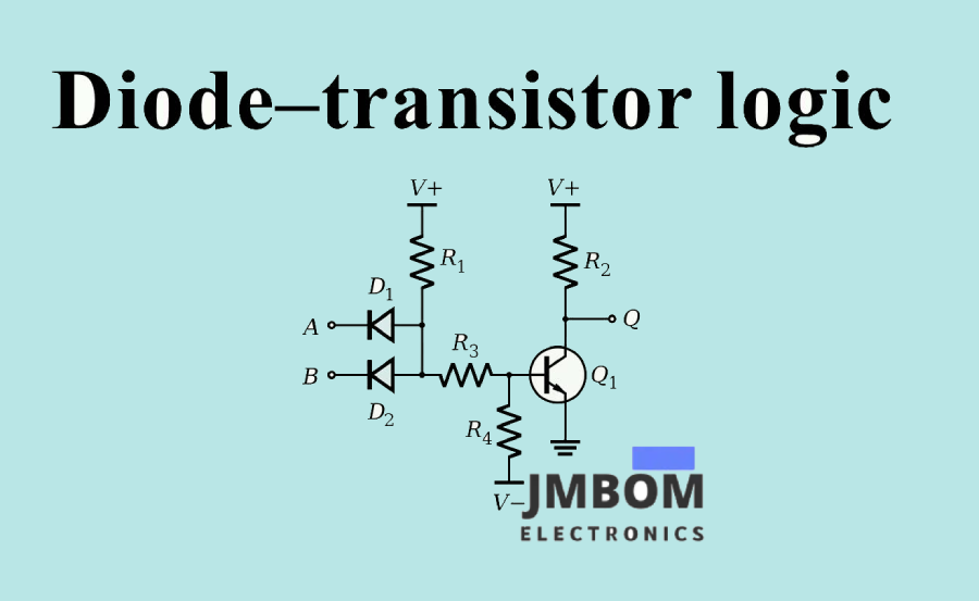
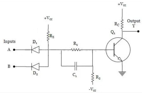
Below is an example of a diode-transistor logic (DTL) circuit configured as a two-input NAND gate. The input section of the circuit consists of two diodes, labeled D1 and D2, along with a resistor R1. These components form the logic input network.
The output stage is built using a transistor Q1 in a common-emitter (CE) configuration and a load resistor R2. Additionally, a capacitor C1 is included in the circuit to supply an overdrive current during switching. This helps reduce the switching time, enhancing the speed of the logic operation.
Diode Transistor Logic NAND Gate
How Diode-Transistor Logic (DTL) Works
When both inputs A and B are LOW, diodes D1 and D2 become forward-biased and start conducting. As a result, current flows from the power supply (+VCC = 5V) through resistor R1 and both diodes to ground. This current causes a voltage drop across R1, reducing the base voltage of transistor Q1. The voltage is not sufficient to turn Q1 ON, so the transistor remains in cut-off mode. In this state, no current flows through the collector, and the output at terminal ‘Y’ stays at a HIGH logic level (Logic 1).
If either input A or B is LOW, the corresponding diode (D1 or D2) is forward-biased, allowing current to flow to ground. This has the same effect: transistor Q1 remains in cut-off mode, and the output at ‘Y’ stays HIGH.
When both inputs A and B are HIGH, diodes D1 and D2 become reverse-biased and stop conducting. In this case, no current flows through the diodes to ground, and the voltage from the +VCC supply is no longer dropped across R1. As a result, the full base voltage reaches transistor Q1, turning it ON (into saturation mode).
Once Q1 conducts, current flows from the collector to the emitter. This causes a significant voltage drop across resistor R2, pulling the output at terminal ‘Y’ down to a LOW level (Logic 0).
Truth Table for Diode-Transistor Logic (DTL)
The truth table for a basic two-input DTL NAND gate is shown below. It illustrates how the output responds to different combinations of logic inputs A and B.
| Input A | Input B | Output Y |
|---|---|---|
| 0 | 0 | 1 |
| 0 | 1 | 1 |
| 1 | 0 | 1 |
| 1 | 1 | 0 |
Propagation Delay in Diode-Transistor Logic (DTL)
One drawback of diode-transistor logic is its relatively high propagation delay. When all inputs are at a HIGH logic level, the transistor enters saturation mode, leading to charge accumulation in the base region. When any input switches to LOW, this stored charge must be removed to turn the transistor off, which increases the delay in signal propagation.
One way to reduce this delay is by placing a capacitor across resistor R3. This capacitor helps to quickly discharge the excess charge from the base, allowing the transistor to switch off faster. Additionally, during the transition to the ON state, the capacitor enhances the base current, helping the transistor turn on more rapidly.
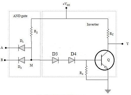
Modified Diode-Transistor Logic Circuit
A modified version of the DTL NAND gate is shown below. In integrated circuit (IC) design, using large-value resistors and capacitors is often impractical due to size and cost constraints. To make the circuit more suitable for IC implementation:
- The capacitor C1 is removed.
- Resistor values are reduced.
- Transistors and diodes are used wherever possible to replace bulky passive components.
This updated DTL design operates with a single positive power supply. The input stage consists of diodes D1 and D2 and resistor R3, forming a basic AND logic function, followed by a transistor-based inverter to complete the NAND gate operation.
Modified DTL
Working of the Modified Diode-Transistor Logic (DTL) Circuit
This modified DTL NAND gate has two input terminals, A and B, which can each be in either a HIGH (logic 1) or LOW (logic 0) state.
Case 1: A = 0, B = 0
When both inputs are LOW, diodes D1 and D2 become forward-biased and conduct. As a result, the voltage at node ‘M’ drops to approximately 0.7 V (the typical forward voltage drop of a diode).
To turn ON transistor Q, a voltage of about 2.1 V is required across the base-emitter path (considering forward drops across D3, D4, and the base-emitter junction). Since the voltage at node M is only 0.7 V, transistor Q remains cut off, and the output Y is pulled up to Vcc, resulting in a HIGH output (Y = 1).
Case 2: A = 0, B = 1 (or A = 1, B = 0)
If one input is LOW and the other is HIGH, one diode (either D1 or D2) will still be forward-biased and conduct, keeping the voltage at node M at approximately 0.7 V. As with the previous case, this is not enough to forward-bias D3, D4, and the base-emitter junction of Q. Therefore, Q remains off, and the output remains HIGH (Y = 1).
Case 3: A = 1, B = 1
When both inputs are HIGH, diodes D1 and D2 are reverse-biased and do not conduct. In this state, current flows through resistor Rd and forward-biased diodes D3 and D4 into the base of transistor Q. This drives Q into saturation, causing the output voltage at Y to drop to LOW (Y = 0).
DTL NOR Gate
Summary of Logic Operation
| Input A | Input B | Output Y |
|---|---|---|
| 0 | 0 | 1 |
| 0 | 1 | 1 |
| 1 | 0 | 1 |
| 1 | 1 | 0 |
Applications of the Modified DTL Circuit
- Higher Fan-Out: The circuit supports higher fan-out since the HIGH output state is maintained with high impedance at the inputs of subsequent gates.
- Improved Noise Immunity: The use of diodes in place of resistors and capacitors enhances the circuit's resistance to electrical noise.
- Cost-Effective for IC Design: Using diodes and transistors instead of large resistors or capacitors simplifies integration and makes the circuit more economical for implementation in integrated circuits.
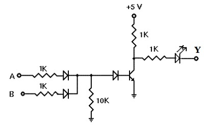
Diode-Transistor Logic (DTL) NOR Gate
The Diode-Transistor Logic NOR gate is constructed similarly to a DTL NAND gate but uses a Diode-Resistor Logic (DRL) OR gate followed by a transistor inverter. A more streamlined way to build a DTL NOR gate is by connecting multiple DTL inverter circuits to a common output. This configuration allows multiple input signals to be combined, effectively forming a NOR logic function.
Diode Transistor Logic AND Gate
To design this circuit, you can use standard components from a typical DTL inverter, including silicon switching diodes such as 1N914 or 1N4148, along with two 4.7 kΩ resistors. The power supply and component values are similar to those used in basic DTL circuits.
Connect the components according to the circuit diagram provided below to complete the NOR gate logic.
Working of the DTL NOR Gate
After assembling the circuit, connect the power supply to it. Then, apply all four possible combinations of inputs A and B using a dip switch or similar input device. For each input combination, observe and record the output logic level at terminal Y, which can be indicated by an LED.
Compare your recorded outputs to the expected results for a NOR gate operation as shown below:
| Input A | Input B | Output Y = (A + B)’ |
|---|---|---|
| 0 | 0 | 1 |
| 0 | 1 | 0 |
| 1 | 0 | 0 |
| 1 | 1 | 0 |
Once all observations are complete, switch off the power supply.
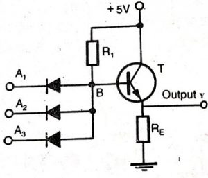
Diode-Transistor Logic (DTL) AND Gate
The DTL AND gate circuit is shown below. In this design, logic 1 corresponds to +5V (positive logic level), while logic 0 corresponds to 0V.
Whenever any one of the inputs A1, A2, or A3 is at a LOW logic level (0), the diode connected to that input becomes forward biased. This causes the transistor to switch off (cut-off mode), resulting in a LOW output (logic 0).
On the other hand, when all three inputs are at HIGH (logic 1), none of the diodes conduct current. This allows the transistor to turn fully ON (saturation mode), producing a HIGH output (logic 1).
Truth Table for Diode-Transistor Logic (DTL) AND Gate
| A1 | A2 | A3 | Output Y = A1 · A2 · A3 |
|---|---|---|---|
| 0 | 0 | 0 | 0 |
| 0 | 0 | 1 | 0 |
| 0 | 1 | 0 | 0 |
| 0 | 1 | 1 | 0 |
| 1 | 0 | 0 | 0 |
| 1 | 0 | 1 | 0 |
| 1 | 1 | 0 | 0 |
| 1 | 1 | 1 | 1 |
Comparison Between DTL, TTL, and RTL Logic Families
| Feature | DTL (Diode-Transistor Logic) | TTL (Transistor-Transistor Logic) | RTL (Resistor-Transistor Logic) |
|---|---|---|---|
| Basic Components | Diodes at input, transistors at output | Bipolar Junction Transistors (BJTs) used throughout | Resistors at input, transistors at output |
| Design | Logic gates built using PN junction diodes and transistors | Logic gates designed mainly with BJTs | Logic gates designed with resistors and transistors |
| Transistor Use | Transistors amplify and switch output signals | One transistor for amplification, another for switching | Transistor used mainly as output device |
| Speed/Response | Faster than RTL | Faster than both DTL and RTL | Slowest among the three |
| Power Loss | Low power loss | Very low power loss | High power loss |
| Circuit Complexity | More complex construction | Simple construction | Simple construction |
| Fan-out (minimum) | 8 | 10 | 5 |
| Power Dissipation per Gate | 8 to 12 mW | 12 to 22 mW | Around 12 mW |
| Noise Immunity | Good | Very good | Medium |
| Propagation Delay | Approximately 30 ns | Between 6 to 12 ns | Around 12 ns |
| Typical Clock Rate | 12 to 30 MHz | 15 to 60 MHz | Around 8 MHz |
| Number of Logic Functions | Fairly high number | Very high number | High number |
| Typical Applications | Basic switching and simple digital circuits | Widely used in modern digital and integrated circuits | Used mainly in early-generation computers |
Advantages of Diode-Transistor Logic (DTL)
- DTL circuits switch faster than Resistor-Transistor Logic (RTL) circuits.
- Using diodes in the input stage makes DTL circuits more cost-effective, as diodes are easier to fabricate on integrated circuits than resistors or capacitors.
- Power loss in DTL circuits is relatively low.
- DTL offers greater fan-out capability and improved noise margin compared to RTL.
Disadvantages of Diode-Transistor Logic
- DTL operates at a slower speed compared to Transistor-Transistor Logic (TTL).
- It suffers from relatively large gate propagation delays.
- At high input levels, the transistor output tends to saturate, which can affect performance.
- DTL circuits generate noticeable heat during operation.
Applications of Diode-Transistor Logic
- DTL is used to design and fabricate digital circuits where diodes form the input logic gates and bipolar junction transistors (BJTs) handle the output stage.
- It is a fundamental logic family for processing electrical signals in digital electronics.
- DTL is commonly employed to build simple logic circuits.
In summary, diode-transistor logic offers improved fan-out and noise margins compared to RTL but operates slower than TTL. While more complex than RTL circuits, DTL replaced RTL in many applications due to its better performance in key areas.
Quick question: Do you know what RTL (Resistor-Transistor Logic) is?
Frequently Ask Questions
What is the difference between a diode and a transistor in logic circuits?
A diode is a two-terminal electronic component that allows current to flow in only one direction. In contrast, a transistor usually has three terminals and can both amplify and switch electronic signals by controlling electron flow through its junctions.
What is diode logic?
Diode logic uses diodes to build basic logic gates that perform Boolean operations. It was commonly used in early computers before transistors replaced vacuum tubes. For example, a diode OR gate outputs logic 1 if any input is 1, while a diode AND gate outputs logic 1 only if all inputs are 1.
Why can't two diodes be used as a transistor?
Two p-n junction diodes connected back-to-back cannot function as a p-n-p transistor because their doping levels are similar. This leads to excessive base current and insufficient collector current, which prevents the transistor action needed for amplification or switching.
Are transistors just logic gates?
Transistors act as electronic switches and amplifiers, which are the fundamental building blocks of most logic gates. Today, the majority of logic gates are implemented using MOSFETs (metal–oxide–semiconductor field-effect transistors) rather than bipolar transistors.
Can you make a transistor from two diodes?
No. Although joining two diodes might create a structure that resembles a transistor, the base region of a real transistor must be very thin and lightly doped—much smaller than the emitter or collector. A transistor is a monolithic device fabricated in a single semiconductor crystal and cannot be constructed simply by connecting two separate diodes.
Does a diode work with AC or DC?
A diode allows current to flow easily in one direction while blocking it in the opposite direction. This property makes diodes useful as rectifiers, which convert alternating current (AC) into pulsating direct current (DC).
Why can't a transistor be used as a rectifier?
Because the transistor's base is very thin and lightly doped, it does not form a proper p-n junction diode suitable for rectification. Therefore, a transistor cannot effectively perform the rectifier function.
Related Articles
Engine Coolant Temperature Sensor: Overview, Function & Circuit Design
Crankshaft Position Sensor: Overview, Circuit Function& Comparison with Camshaft Sensors
Inverting Summing Amplifier: Circuit Diagram,Operation and Formula
Active Bandpass Filter: Overview, Types,Q Factor & Applications
Passive High-Pass Filter: Overview, Circuit Design & Transfer Function
Differential Pressure Sensors: Working Principle, Interfacing,Testing Methods and Common Issues
Voltage Amplifier: Circuit Design, Gain, vs. Power Amplifier, and Key Applications
Resistor-Transistor Logic (RTL):Operation, Features, and Applications

Amanda Miller
Amanda Miller is a senior electronics engineer with 6 years of experience. She focuses on studying resistors, transistors, and package design in detail. Her deep knowledge helps her bring innovation and high standards to the electronics industry.
Subscribe to JMBom Electronics !


